Device for improving gate driving capability and manufacturing method thereof
A technology of gate drive and manufacturing method, which is applied in semiconductor/solid-state device manufacturing, semiconductor devices, electric solid-state devices, etc., can solve problems such as increased switching loss, insufficient IC drive capability, and device inoperability, so as to avoid slow turn-on Effect
- Summary
- Abstract
- Description
- Claims
- Application Information
AI Technical Summary
Problems solved by technology
Method used
Image


Examples
Embodiment Construction
[0036] The present invention is further illustrated below in conjunction with the accompanying drawings and specific embodiments. The present embodiment is implemented on the premise of the technical solution of the present invention. It should be understood that these embodiments are only used to illustrate the present invention and not to limit the scope of the present invention.
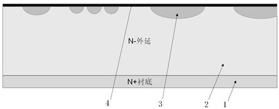
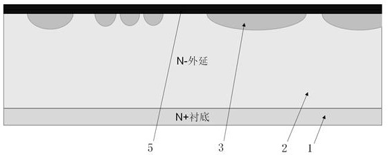
[0037] like Figures 1 to 8 As shown, an embodiment of the present invention provides a method for fabricating a device with improved gate driving capability, including:
[0038] see figure 1 , an N-type substrate 1 is provided, and an epitaxial layer 2 is fabricated on the upper side of the substrate 1 . The substrate 1 is generally doped with arsenic or antimony. By choosing different resistivity and thickness of the epitaxial layer 2, different device withstand voltages can be obtained. Usually, the thickness of the epitaxial layer 2 is 40-80um, and the resistivity of the epitaxial layer is ...
PUM
| Property | Measurement | Unit |
|---|---|---|
| thickness | aaaaa | aaaaa |
| thickness | aaaaa | aaaaa |
| thickness | aaaaa | aaaaa |
Abstract
Description
Claims
Application Information