High-brightness external cavity semiconductor laser

A laser and high-brightness technology, applied in the laser field, can solve the problems of increased beam parameter product and poor brightness effect

Pending Publication Date: 2022-07-22
BWT BEIJING
View PDF5 Cites 1 Cited by
  • Summary
  • Abstract
  • Description
  • Claims
  • Application Information

AI Technical Summary

Problems solved by technology

[0004] In the process of realizing the present invention, the inventor found that there are at least the following problems in the prior art: the prior art can arrange the beams of multiple laser tubes side by side. The spot is larger than that of a single laser and a single tube, and the beam parameter product (the product of the waist spot size and the far-field divergence angle) will increase accordingly. The energy radiated in the beam parameter product, so the effect of the existing technology to improve the brightness is not good

Method used


Image

  • High-brightness external cavity semiconductor laser
  • High-brightness external cavity semiconductor laser
  • High-brightness external cavity semiconductor laser

Examples


Embodiment Construction

[0031] The following describes in detail the embodiments of the present invention, examples of which are illustrated in the accompanying drawings, wherein the same or similar reference numerals refer to the same or similar elements or elements having the same or similar functions throughout. The embodiments described below with reference to the accompanying drawings are exemplary, only used to explain the present invention, and should not be construed as a limitation of the present invention. On the contrary, embodiments of the present invention include all changes, modifications and equivalents falling within the spirit and scope of the appended claims.

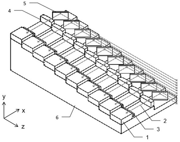
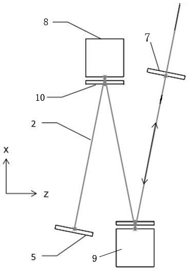
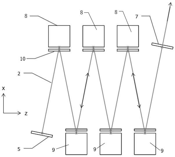
[0032] figure 2 It is a schematic structural diagram of a high-brightness external cavity semiconductor laser proposed by an embodiment of the present invention.

[0033] see figure 2 , a high-brightness external cavity semiconductor laser, including an external cavity, the external cavity includes a first laser single t...


PUM


Abstract

The invention provides a high-brightness external cavity semiconductor laser which comprises an external cavity, and the external cavity comprises a first laser single tube, a second laser single tube and an external cavity mirror. The first end of the first laser single tube and the first end of the second laser single tube are oppositely arranged, and the axis of the first laser single tube and the axis of the second laser single tube are not collinear; through adjustment of the outer cavity mirror, light beams emitted by the first laser single tube and the second laser single tube are subjected to turn-back oscillation in the outer cavity, coherent beam combination is carried out, and laser is output through the outer cavity mirror. The cost is low, the high-power laser beam can be obtained, the overall beam is kept close to the beam parameter product of one laser single tube, the laser beam quality is kept, and the brightness of the laser beam can be improved.

Description

technical field [0001] The invention relates to the field of laser technology, in particular to a high-brightness external cavity semiconductor laser. Background technique [0002] Since the advent of semiconductor lasers, they have been more and more widely used in precision measurement and Materials processing, communications and many other fields. [0003] One solution to increasing the high power and brightness required by semiconductor lasers is spatial beam combining. refer to figure 1 , in the prior art, the space beam combining needs to use a base plate 6 with a stepped structure, so that the beams output by the single laser tubes 1 pass through the fast-axis collimating lens 3 and the slow-axis collimating lens 4 in sequence. Multiple single laser tubes are arranged in sequence in space to form a larger spot. [0004] In the process of realizing the present invention, the inventor found that there are at least the following problems in the prior art: the prior a...

Claims


Application Information

Patent Timeline
Patent Type & Authority Applications(China)
IPC IPC(8): H01S5/14H01S5/40
CPCH01S5/14H01S5/4018H01S5/4012
Inventor 陈晓华郭渭荣王宝华时敏李娟董晓培郭方君玥
Owner BWT BEIJING
Why Eureka
Try Eureka