Supercharge Your Innovation With Domain-Expert AI Agents!

Chip internal image processing architecture and image processing method

An image processing and chip technology, applied in image communication, color signal processing circuits, components of color TV, etc., can solve the problem of high use cost, and achieve the effect of reducing chip area and use cost

Pending Publication Date: 2022-07-22
AMICRO SEMICON CORP
View PDF0 Cites 0 Cited by
  • Summary
  • Abstract
  • Description
  • Claims
  • Application Information

AI Technical Summary

Problems solved by technology

In future applications, the complexity of the system will become higher and higher, and the demand for cameras will increase. The chip needs to support multiple cameras, while the existing internal image processing architecture of a single chip only supports a single camera. When using multiple cameras , requires multiple image processing architectures for image processing, and the use cost is high

Method used


Image

  • Chip internal image processing architecture and image processing method
  • Chip internal image processing architecture and image processing method

Examples


Embodiment Construction

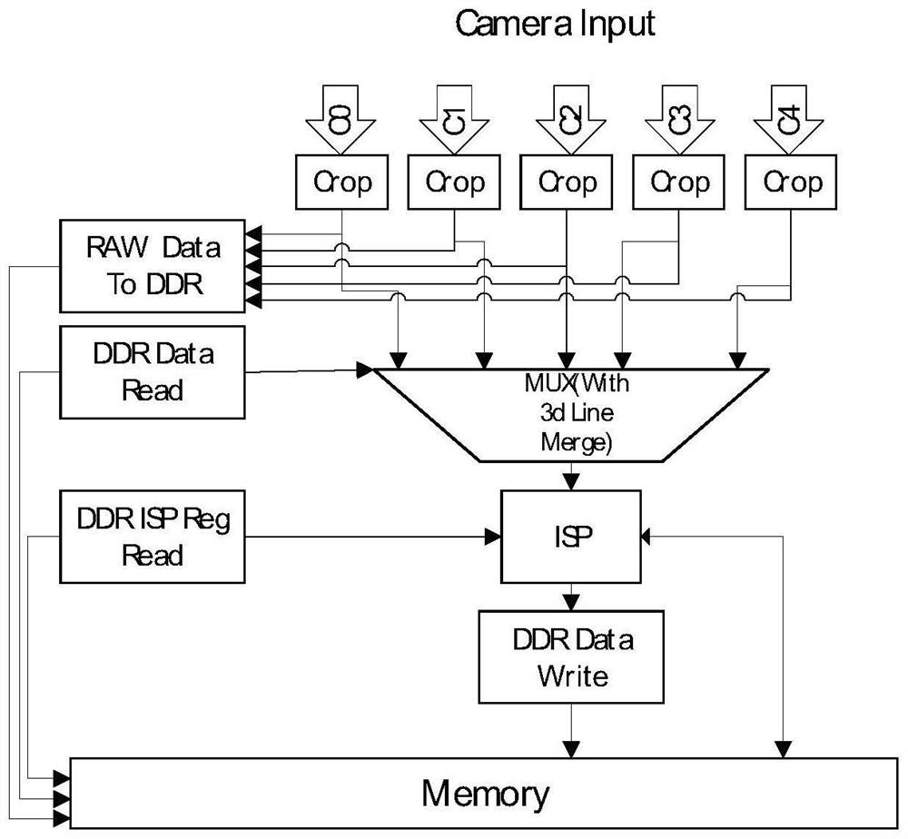
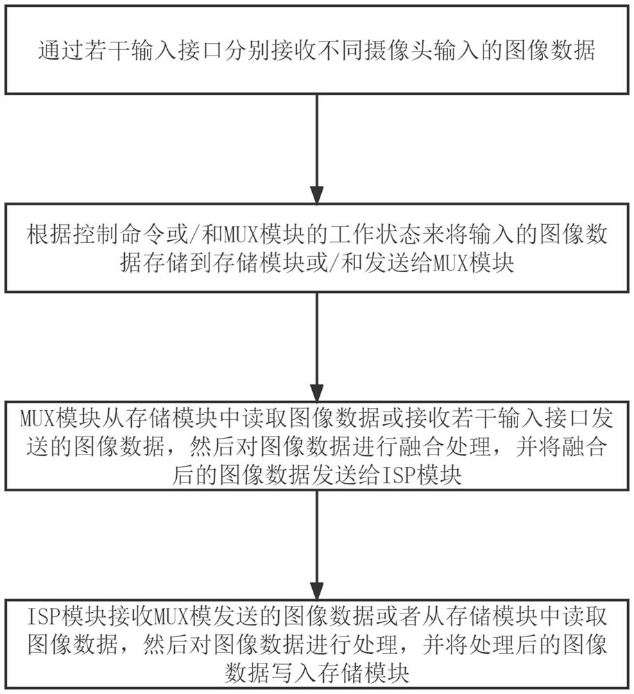
[0017] The following describes in detail the embodiments of the present invention, examples of which are illustrated in the accompanying drawings, wherein the same or similar reference numerals refer to the same or similar elements or elements having the same or similar functions throughout.

[0018] In the description of the present invention, it should be noted that, for orientation words, such as the terms "center", "horizontal", "longitudinal", "length", "width", "thickness", "upper", "lower" , "Front", "Back", "Left", "Right", "Vertical", "Horizontal", "Top", "Bottom", "Inside", "Outside", "Clockwise", "Counterclockwise" ” and the like indicating the orientation and positional relationship are based on the orientation or positional relationship shown in the accompanying drawings, which are only for the convenience of describing the present invention and simplifying the description, rather than indicating or implying that the referred device or element must have a specific ...


PUM


Abstract

The invention discloses a chip internal image processing architecture and an image processing method. The chip internal image processing architecture comprises an MUX module, an ISP module, a storage module and a plurality of input interfaces. The plurality of input interfaces are connected with the storage module and are used for storing image data input by different cameras into the storage module; the MUX module is respectively connected with the storage module, the ISP module and the plurality of input interfaces, and is used for receiving the image data from the plurality of input interfaces or reading the image data from the storage module to carry out image data fusion processing, and then sending the fused image data to the ISP module; the ISP module is connected with the MUX module and used for receiving image data spliced by the MUX module, and the ISP module is connected with the storage module and used for reading the image data from the storage module or writing the image data into the storage module. The chip is enabled to support multiple cameras, the area of the chip is reduced, and the use cost is reduced.

Description

technical field [0001] The invention relates to the technical field of chips, in particular to an image processing architecture and an image processing method inside a chip. Background technique [0002] The camera is an image-based sensor, which plays a very important role in robot perception. Image information contains a large amount of data information, and the potential of image information is constantly being tapped through algorithms. In future applications, the system complexity will become higher and higher, and the demand for cameras will increase. The chip needs to support multiple cameras, and the existing image processing architecture inside a single chip only supports a single camera. When using multiple cameras , requires multiple image processing architectures for image processing, and the use cost is high. SUMMARY OF THE INVENTION [0003] In order to solve the above problems, the present invention provides an internal image processing architecture and an ...

Claims


Application Information

Patent Timeline
IPC IPC(8): H04N5/14H04N5/217H04N5/235H04N5/265H04N5/76H04N9/64H04N9/73
CPCH04N5/14H04N5/265H04N5/76H04N9/64H04N23/81H04N23/70H04N23/88
Inventor 赖钦伟
Owner AMICRO SEMICON CORP
Features
  • R&D
  • Intellectual Property
  • Life Sciences
  • Materials
  • Tech Scout
  • Unparalleled Data Quality
  • Higher Quality Content
  • 60% Fewer Hallucinations
Learn More