Method for forming self-aligning contact structure in semiconductor IC device

A self-aligned contact, integrated circuit technology, used in semiconductor devices, semiconductor/solid-state device manufacturing, electrical solid-state devices, etc., can solve reliability problems and other issues

Inactive Publication Date: 2004-05-26
SAMSUNG ELECTRONICS CO LTD
View PDF1 Cites 0 Cited by
  • Summary
  • Abstract
  • Description
  • Claims
  • Application Information

AI Technical Summary

Problems solved by technology

[0006] Therefore, the self-aligned contact hole fabrication technique still has reliability problems when using photolithographic alignment techniques with large alignment errors

Method used


Image

  • Method for forming self-aligning contact structure in semiconductor IC device
  • Method for forming self-aligning contact structure in semiconductor IC device
  • Method for forming self-aligning contact structure in semiconductor IC device

Examples


Embodiment Construction

[0014] The present invention will now be described in more detail with reference to the accompanying drawings showing preferred embodiments of the invention. However, the present invention can be implemented in various ways and should not be limited to the embodiments presented here. Rather, these embodiments are provided so that this disclosure will be thorough and complete, and will fully convey the scope of the invention to those skilled in the art. In the drawings, the thickness of layers and regions are exaggerated for clarity. It will also be understood that when a layer is referred to as being "on" another layer or substrate, it can be directly on the other layer or substrate, or intervening layers may also be present. Like numbers indicate like elements throughout the several drawings.

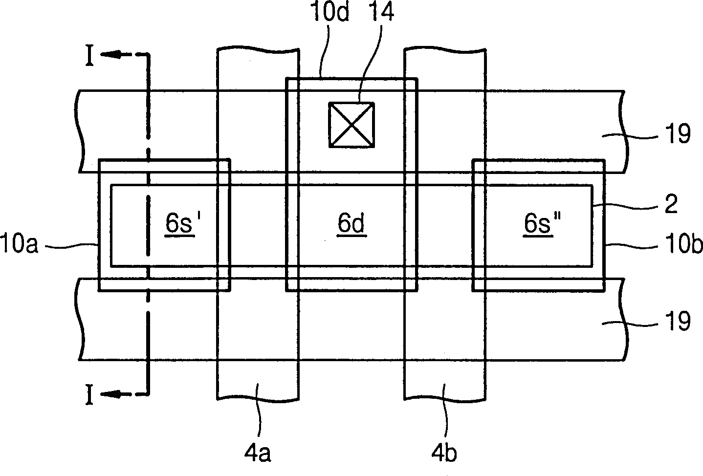
[0015] figure 1 A top view of a portion of a typical DRAM cell array area.

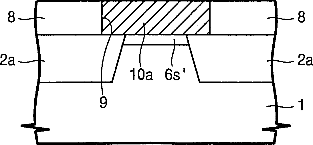
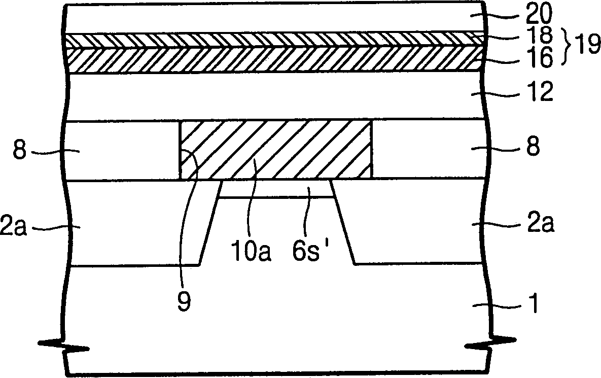
[0016] refer to figure 1 , the active region 2 is defined in a predetermined region of the P-type semi...


PUM


Abstract

Methods of forming integrated circuit devices include the use of preferred self-aligned contact hole fabrication steps. These steps improve process reliability. A plurality of line patterns are formed on a substrate. A capping insulating layer is formed to cover the surface of the line patterns and the surface of the substrate. An upper interlayer insulating layer is formed on the capping insulating layer to fill a gap region between the line patterns. The upper interlayer insulating layer and the capping insulating layer are patterned, so that the first contact hole is formed between the line patterns. By wet-etching the upper interlayer insulating layer selectively, the first contact hole is extended, so that the second contact hole for exposing the capping insulating layer on the sidewall of the line patterns is formed.

Description

technical field [0001] This application is based on the priority of Korean Patent Application No. 2000-05358 filed on February 3, 2000, the contents of which are incorporated herein by reference. Background technique [0002] The present application relates to methods of manufacturing integrated circuit devices, and more particularly to methods of forming self-aligned contact structures in semiconductor integrated circuit devices. [0003] Attempts to increase integration density in microelectronic integrated circuits have generally resulted in the fabrication of smaller and more closely spaced devices. In order to access these devices, the conventional technique of defining the location of contact holes for these devices using photolithographic processes must be improved. Such improvements typically include the development of lithographic alignment techniques that reduce errors. Furthermore, when forming highly integrated devices, attempts to reduce contact hole size have...

Claims


Application Information

Patent Timeline
Patent Type & Authority Patents(China)
IPC IPC(8): H01L21/28H01L21/60H01L21/768H01L21/82H01L21/8242H01L27/108
CPCH01L21/76897H01L27/10885H01L27/10855H01L21/76831H10B12/0335H10B12/482H01L21/82
Inventor 朴钟佑金允基朴东建
Owner SAMSUNG ELECTRONICS CO LTD
Why Eureka
Try Eureka