Display panel
A display panel and image display technology, which is applied in the direction of instruments, printed circuits connected with non-printed electrical components, electrical components, etc., can solve the problem of increased resistance of wiring lines 10, difficulty in using power lines, and failure of semiconductor integrated circuits and other issues to achieve the effect of easy installation and cost reduction
- Summary
- Abstract
- Description
- Claims
- Application Information
AI Technical Summary
Problems solved by technology
Method used
Image

Examples
Embodiment 1
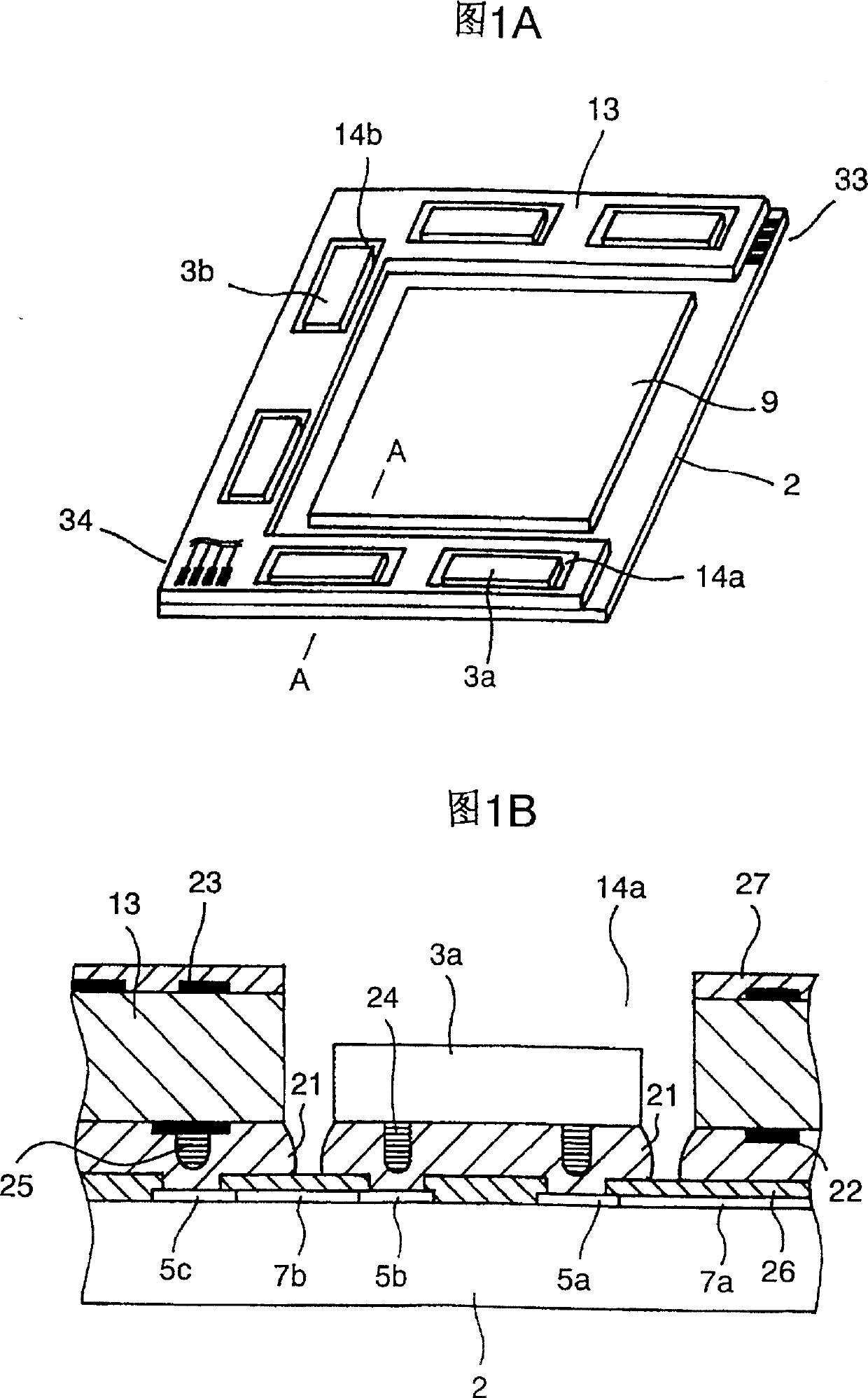
[0050] As shown in FIGS. 1A and 1B, an active substrate 2 includes a terminal electrode 5a, a wiring line 7a for connecting the terminal electrode 5a to a signal line, and a wiring line 7a for connecting the terminal electrode 5b. , 5c wiring line 7b.
[0051]Preferably, these terminal electrodes 5a, 5b, 5c and wiring lines 7a, 7b should be formed at the same time.
[0052] An insulating layer 26 includes a gate insulating layer, a passivation (passivation) insulating layer, and other insulating layers formed on the main surface of the active substrate 2, and selectively removes the upper surfaces of the terminal electrodes 5a, 5b, 5c The upper insulating layer, while exposing the surface of each electrode.
[0053] At the mounting surface side of the driver IC chip 3a electrically connected to the terminal electrodes 5a, 5b, a bump electrode 24 electrically connected to the terminal electrodes 5a, 5b is formed.
[0054] In the printed circuit 13 that is electrically connect...
Embodiment 2
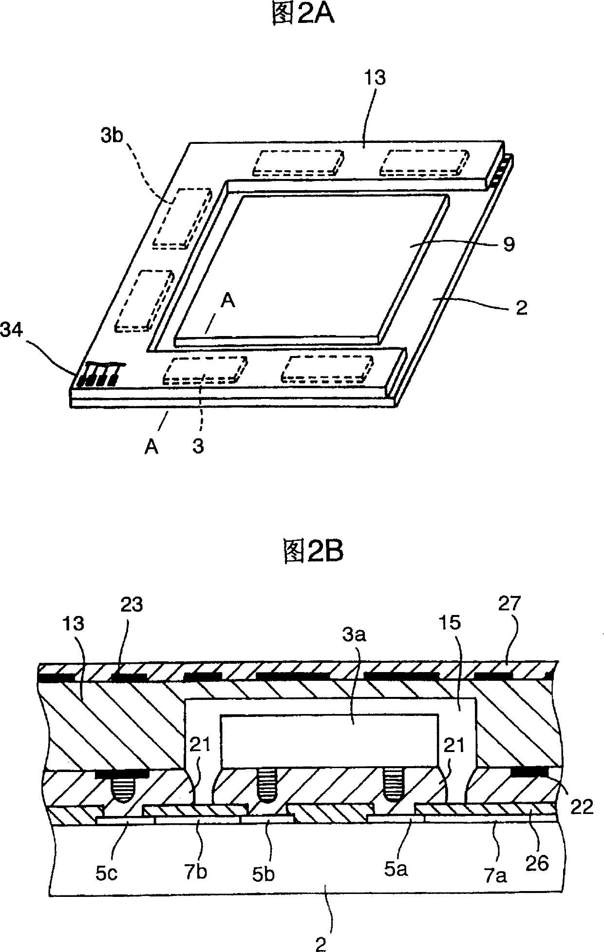
[0066] Embodiment 1 above employs the printed circuit board 13 in which the openings 14a, 14b are formed at positions corresponding to the mounting positions of the driver integrated circuit chips 3a, 3b. In Embodiment 2, it is intended to use a printed circuit board 13 having a deep recess 15 larger than the outline of the driver integrated circuit chips 3a, 3b while covering the driver integrated circuit chips 3a, 3b mounted on the active substrate 2. 3b's upper surface. This embodiment has the same effect as Embodiment 1.
[0067] Also in this embodiment, in the same manner as in Embodiment 1, it is not necessary to use a conventional long bus flexible film, and the cost is reduced. However, in Embodiment 1, the thick wiring lines 22 , 23 formed on both sides of the printed circuit board 13 have limitations in circuit design in order to narrow the line width or reduce the number of lines near the opening 14 . However, the printed circuit board 13 in Embodiment 2 is exempt...
Embodiment 3
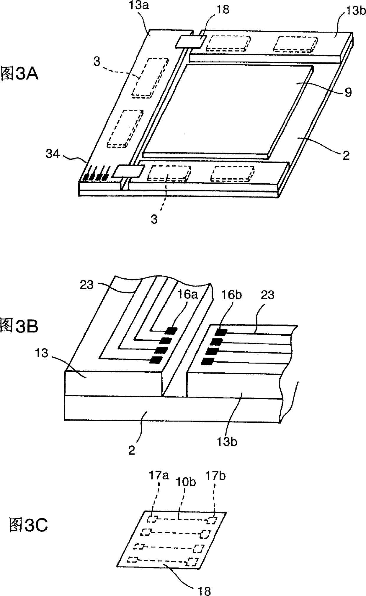
[0070] Fig. 3 explains Embodiment 3 of the present invention.
[0071] Fig. 3A is a perspective view of a liquid crystal panel, Fig. 3B is a substantially enlarged view thereof, and Fig. 3C shows a connecting film for joining split circuit boards together.
[0072] Embodiments 1 and 2 above present the L-shaped or π-shaped printed circuit board 13 integrating a printed circuit board connected to the connection terminals of the scanning lines and a printed circuit board connected to the connection terminals of the signal lines. Even when such a printed circuit board 13 is used, in a small-sized liquid crystal panel of size 3 (diagonal 7.5 cm) or smaller, when the printed circuit board 13 is mounted, due to a temperature rise between the printed circuit board 13 and the active The expansion difference between the substrates 2 is also small, and the material cost and processing cost of the printed circuit board 13 are small and hardly problematic.
[0073] However, in general, a...
PUM
| Property | Measurement | Unit |
|---|---|---|
| thickness | aaaaa | aaaaa |
| length | aaaaa | aaaaa |
| thickness | aaaaa | aaaaa |
Abstract
Description
Claims
Application Information
 - R&D Engineer
- R&D Manager
- IP Professional
- Industry Leading Data Capabilities
- Powerful AI technology
- Patent DNA Extraction
Browse by: Latest US Patents, China's latest patents, Technical Efficacy Thesaurus, Application Domain, Technology Topic.
© 2024 PatSnap. All rights reserved.Legal|Privacy policy|Modern Slavery Act Transparency Statement|Sitemap