Power semiconductor device

A technology of power semiconductors and semiconductors, which is applied in the direction of semiconductor devices, semiconductor/solid-state device manufacturing, and electric solid-state devices, and can solve problems such as deterioration of performance-price ratio

Inactive Publication Date: 2004-08-18
KK TOSHIBA
View PDF0 Cites 2 Cited by
  • Summary
  • Abstract
  • Description
  • Claims
  • Application Information

AI Technical Summary

Problems solved by technology

[0008] However, in the case of adopting the above-mentioned

Method used


Image

  • Power semiconductor device
  • Power semiconductor device
  • Power semiconductor device

Examples


Embodiment Construction

[0013] Hereinafter, embodiments of the present invention will be described with reference to the drawings.

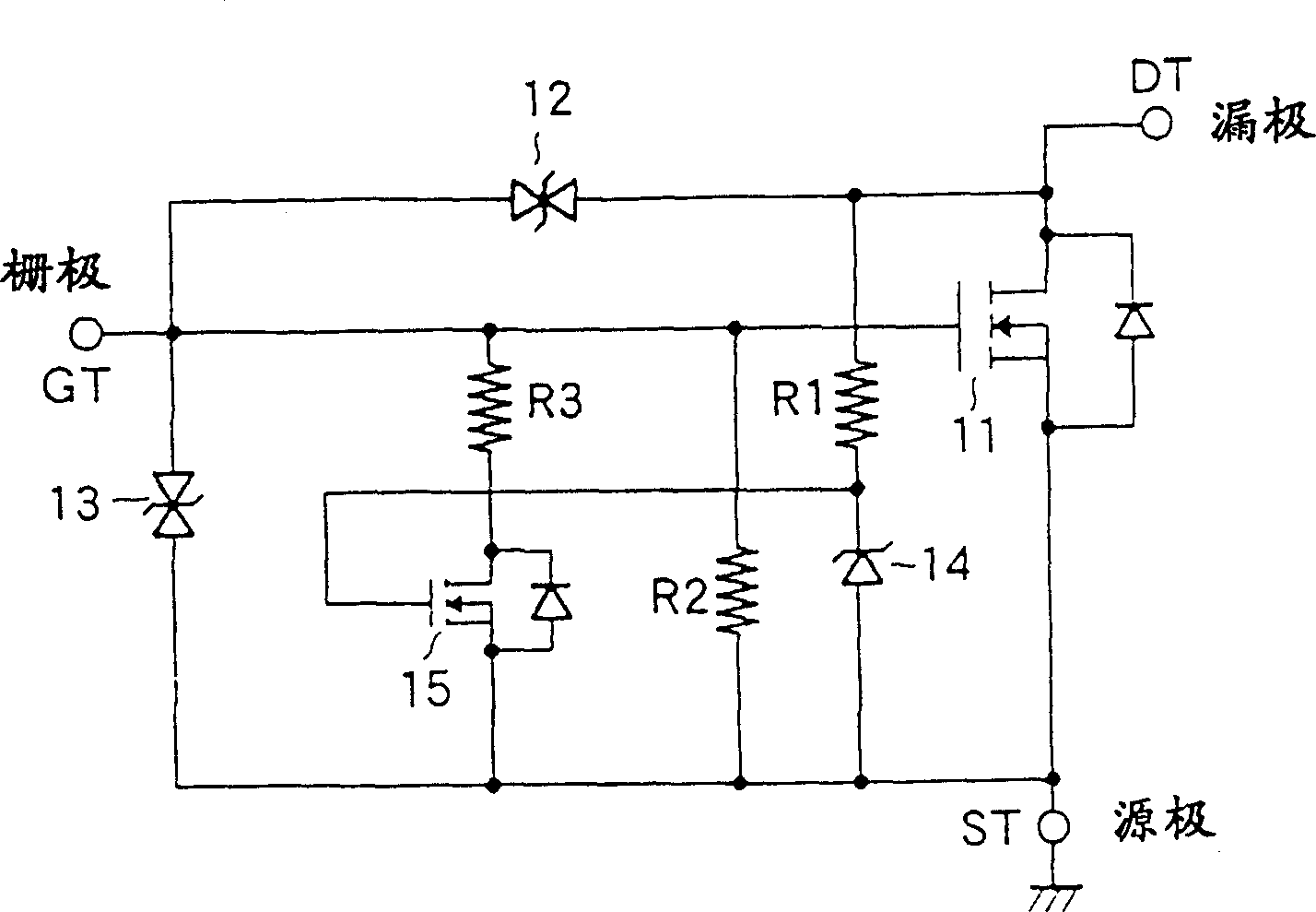
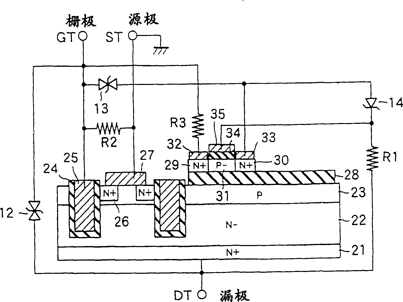
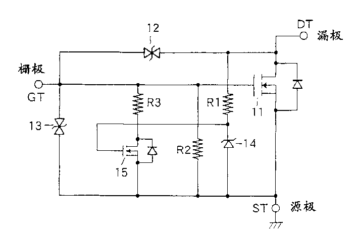
[0014] figure 1 The circuit diagram of is showing the constitution of the power semiconductor device of the embodiment of the present invention.

[0015] The power semiconductor device consists of an n-channel power metal-oxide-semiconductor field-effect transistor (MOS field-effect transistor) 11, an active clamp diode 12, a gate protection diode 13, a Zener diode 14, and a lateral n-channel MOS transistor. 15 and resistance R1, R2, R3 form.

[0016] The drain terminal DT is connected to the drain of the metal oxide semiconductor field effect transistor 11, and the gate of the metal oxide semiconductor field effect transistor 11 and the source of the metal oxide semiconductor field effect transistor 11 are respectively connected to Gate terminal GT and source terminal ST.

[0017] An active clamp diode 12 is connected between the drain terminal DT and the gate termi...


PUM


Abstract

The present invention provides a power semiconductor device which can prevent the thermal breakdown of a power MOSFET when the gate potential of the power MOSFET is not fixed. The power semiconductor device comprises a power MOSFET 11, a series resistor R1 and Zener diode 14 connected between the drain and the source of the power MOSFET 11, a resistor R2 connected between the gate and the source of the power MOSFET 11, and a series resistor R3 and MOS transistor 15 connected between the gate and the source of the power MOSFET 11. The joint of the resistor R1 and the Zener diode 14 is connected to the gate of the MOS transistor 15.

Description

technical field [0001] The present invention relates to a power semiconductor device, in particular to a voltage-driven power metal oxide semiconductor field effect transistor for power. Background technique [0002] The above-mentioned voltage-driven metal oxide semiconductor field effect transistor (MOS field effect transistor) is generally used as a switch for driving a motor. For example, switches for driving ABS pump motors for vehicles are typical applications. [0003] In the switch for driving the pump motor described above, in general, a control IC for controlling the gate potential is mounted on the gates of a plurality of metal oxide semiconductor field effect transistors. Then, a pump motor drive circuit including this switch is constructed. In addition, there are IPD (Intelligent Power Device, Intelligent Power Device) and IPM (Intelligent Power Module, Intelligent Power Module) with built-in IC for control. [0004] Conventionally, in such a circuit configur...

Claims


Application Information

Patent Timeline
IPC IPC(8): H01L27/088H01L21/8234H01L27/02H01L27/04H01L27/06H01L29/78H01L29/786H03K17/082
CPCH01L27/0251H01L27/0629H01L29/7803H03K17/0822H01L29/7813H01L29/78
Inventor 米田辰雄
Owner KK TOSHIBA
Why Eureka
Try Eureka