Eureka AIR delivers breakthrough ideas for toughest innovation challenges, trusted by R&D personnel around the world.

Technology for producing semiconductor device

A semiconductor and device technology, applied in the field of semiconductor device production, can solve problems such as chip breakage, effort, and time-consuming

Inactive Publication Date: 2004-09-22
LINTEC CORP
View PDF0 Cites 0 Cited by
  • Summary
  • Abstract
  • Description
  • Claims
  • Application Information

AI Technical Summary

Problems solved by technology

However, in this method, the film adhesive needs to be cut into substantially the same shape as the chip in advance, so implementing this method is time-consuming
Also, the bonding work of the film adhesive having an extremely small size as the chip is essential, so this method is laborious
[0009] Even if any of the above methods are used, it is still necessary to deal with the tiny chips that have been ground to a very small thickness and become very fragile and fragile, so a slight misuse will cause the chips to break

Method used


Image

  • Technology for producing semiconductor device
  • Technology for producing semiconductor device
  • Technology for producing semiconductor device

Examples


example 1

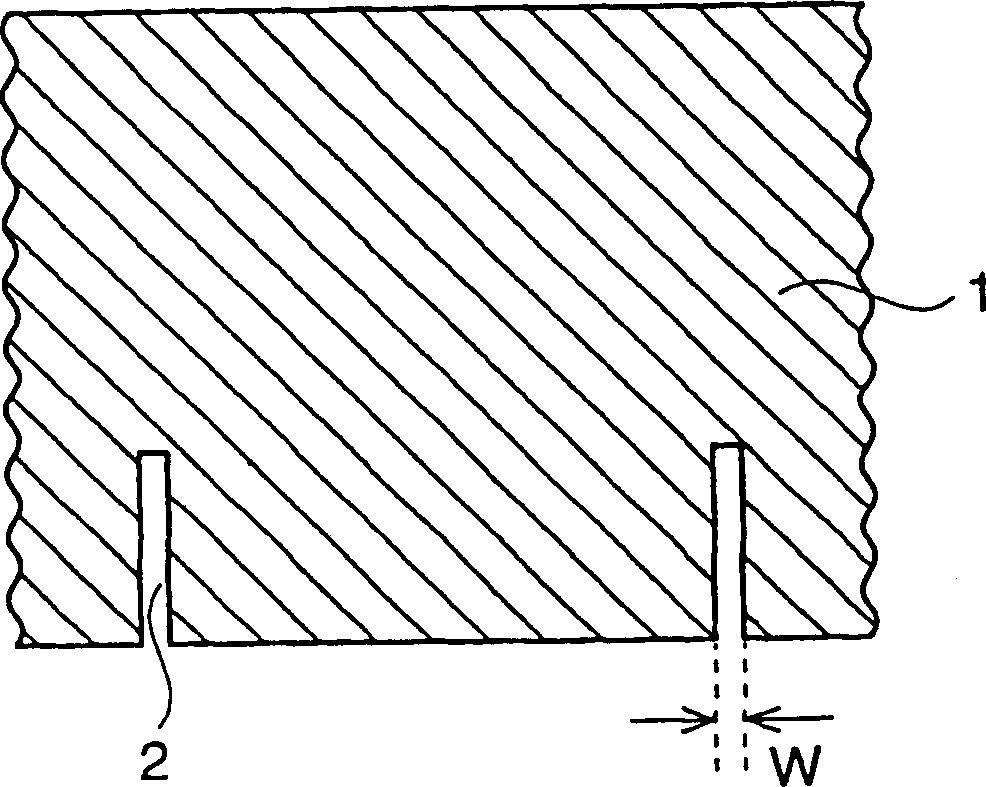
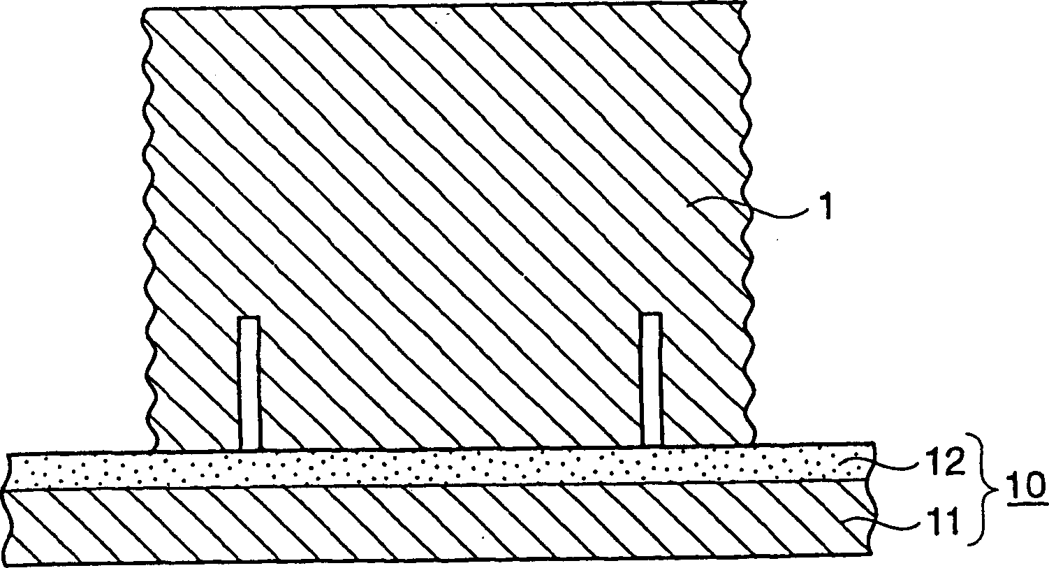
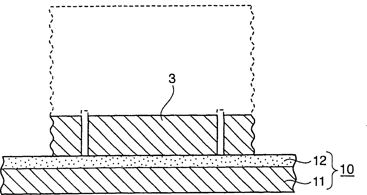
[0072] A silicon wafer with a diameter of 6 inches and a thickness of 700 μm was glued to a dicing tape (Adwill D-628), using a wafer slicer (DAD 2H / 6T, manufactured by Disco Corporation) with a blade width of 35 μm, at a cutting depth of 400 μm and Grooves were formed under the condition that the chip size was 6 mm2. Subsequently, a thin layer of surface protection is adhered to the grooved surface of the wafer. The dicing tape was peeled off, and the back surface of the wafer was ground using a back grinder (DFG 840, manufactured by Disco Corporation) until its thickness became 80 μm, thereby achieving separation of the wafer into individual chips. Thereafter, a dicing / die-bonding sheet (Adwill LE5000) was adhered to the ground backside of the wafer (chip), irradiated with ultraviolet light and the surface protective sheet was peeled off. The slice / die-bonding thin layer was irradiated with ultraviolet light, and the adjacent segments located in the divided sections were cu...

example 2

[0075] A silicon wafer with a diameter of 6 inches and a thickness of 700 μm is glued to a dicing tape (Adwill D-628), using a wafer slicer (DAD 2H / 6T, manufactured by Disco Corporation) with a blade width of 35 μm, at a cutting depth of 400 μm and Grooves were formed under the condition that the chip size was 5 mm2. Subsequently, a thin layer of surface protection is adhered to the grooved surface of the wafer. The dicing tape was peeled off, and the back surface of the wafer was ground using a back grinder (DFG 840, manufactured by Disco Corporation) until its thickness became 80 μm, thereby achieving separation of the wafer into individual chips. Thereafter, the dicing / die-bonding thin layer (thermoplastic polyimide film) is heated at about 130°C and adhered to the ground backside of the wafer (chip), and the surface protective thin layer is peeled off. Using a wafer slicer (DAD 2H / 6T, manufactured by Disco Corporation) with a blade width of 30 μm, the adhesive layer betwe...


PUM


Abstract

A process for producing a semiconductor device, comprising the steps of providing a wafer of given thickness having a surface furnished with semiconductor circuits and a back; forming grooves of a cut depth smaller than the thickness of the wafer, said grooves extending from the wafer circuit surface; sticking a surface protective sheet onto the wafer circuit surface; grinding the back of the wafer so that the thickness of the wafer is reduced to thereby finally result in division of the wafer into individual chips with spaces therebetween; sticking a dicing / die bond sheet onto the ground back of the wafer, said dicing / die bond sheet comprising a base and, superimposed thereon, an adhesive layer, said adhering performed so that the adhesive layer is brought into contact with the ground back of the wafer; peeling the surface protective sheet from the wafer circuit surface to thereby cause the adhesive layer of the dicing / die bond sheet to be exposed through each space between neighboring individual chips; cutting the exposed adhesive layer of the dicing / die bond sheet; detaching the individual chips having the cut adhesive layer adhering thereto from the base of the dicing / die bond sheet; and bonding the individual chips through the adhesive layer to a given substrate. This process is advantageous in that an appropriate amount of adhesive layer can easily be formed on the back of extremely thin chips to thereby enable avoiding chip breakage, chip cracking or package cracking, so that a productivity enhancement can be realized.

Description

technical field [0001] The present invention relates to the production of semiconductor devices. In particular, the present invention relates to a method for producing a semiconductor device in which an appropriate amount of an adhesive layer can be easily formed on an extremely thin chip backside so that chip breakage, chip cracking or package cracking can be avoided, so that improvement in productivity can be achieved . Background technique [0002] In recent years, the spread of IC cards has been promoted, and further reduction in thickness thereof is now required. Correspondingly, the thickness of the semiconductor chip, which is now required to be about 350 μm, is reduced to 50-100 μm or even less. [0003] Thin semiconductor chips can be obtained by first sticking a surface protection tape for back grinding to the circuit surface of the wafer, then grinding the back side of the wafer, and thereafter dicing the wafer. When the thickness of the wafer becomes extremely...

Claims


Application Information

Patent Timeline
IPC IPC(8): H01L23/12H01L21/301H01L21/304H01L21/52H01L21/58H01L21/68H01L21/78
CPCH01L2924/01082H01L2221/68327H01L2924/01004H01L2924/01045H01L21/6836H01L2924/01027H01L21/3043H01L2924/01013H01L2924/014H01L2224/8385H01L2224/274H01L2224/83191H01L2924/0665H01L2224/2919H01L24/27H01L2924/10158H01L21/78H01L2224/743H01L2924/14H01L24/83H01L24/743H01L2924/01005H01L24/29H01L2924/01033H01L2924/01006H01L2924/01074H01L2924/10253H01L2924/01075H01L2924/07802H01L2924/12044H01L2924/00H01L2924/3512
Inventor 杉野贵志妹尾秀男
Owner LINTEC CORP
Why Eureka
Eureka Blog
Learn More