Check patentability & draft patents in minutes with Patsnap Eureka AI!

Bidirectional ESD diode structure

A bidirectional diode, electrostatic discharge technology, applied in diodes, circuits, transistors, etc., can solve problems such as reducing the degree of ESD protection

Inactive Publication Date: 2005-01-05
NXP BV
View PDF0 Cites 2 Cited by
  • Summary
  • Abstract
  • Description
  • Claims
  • Application Information

AI Technical Summary

Problems solved by technology

Reducing the size or area of ​​the diode can reduce the junction capacitance, but since the degree of ESD protection depends on the current density in the diode, this in turn will reduce the degree of ESD protection

Method used


Image

  • Bidirectional ESD diode structure
  • Bidirectional ESD diode structure
  • Bidirectional ESD diode structure

Examples


Embodiment Construction

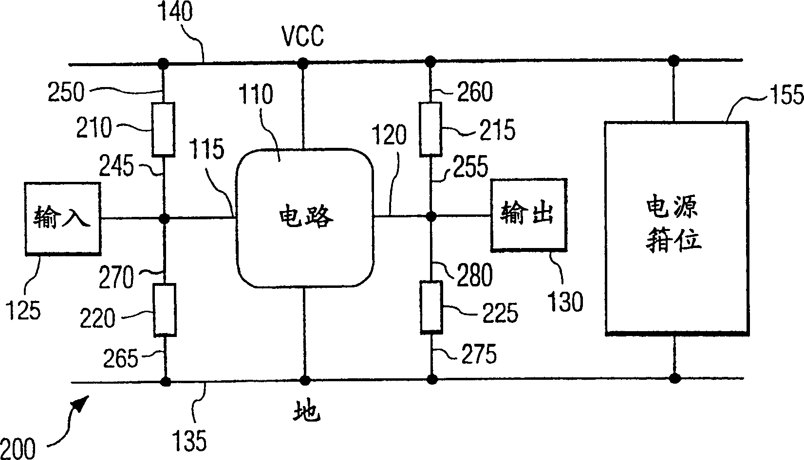
[0033] figure 2 A circuit arrangement 200 is shown in which the diodes D1-D4 shown in FIG. 1 are replaced by devices which provide improved electrostatic discharge (ESD) protection. Specifically, diodes D1 , D2 , D3 , D4 are replaced by two-terminal network-integrated structures called ESD diodes 210 , 215 , 220 , 225 , respectively.

[0034] Anode 245 of ESD diode 210 and anode 255 of ESD diode 215 are connected to input 115 and output 120 of circuit 110 , respectively. The cathodes 250 , 260 of the ESD diodes 210 , 215 are connected to the power bus 140 . In addition, the cathode 270 of the ESD diode 220 and the cathode 280 of the ESD diode 225 are connected to the input terminal 115 and the output terminal 120 of the circuit 110, respectively. The anodes 265 , 275 of the ESD diodes 220 , 225 are connected to the ground bus 135 , which may be replaced by a bus on which a lower voltage than the supply bus 140 provides. As an example, the power supply bus 140 voltage is a ...


PUM


Abstract

A bi-directional ESD diode protects a circuit against electrostatic discharge (ESD). The bi-directional diode has a first device and a second device, each including a first region and a third region formed by doping a semiconductor substrate so that it has a P-type conductivity; and a second region and a fourth region formed by doping the semiconductor substrate so that it has an N-type conductivity. The first region of the first device and the fourth region of the second device are for connection to an anode terminal of the bi-directional diode. The fourth region of the first device and the first region of the second device are for connection a cathode terminal of the bi-directional diode. The anode terminal is for connection to a signal terminal of the circuit when the cathode terminal is connected to a positive power line of the circuit, and the cathode terminal is for connection to the signal terminal when the anode terminal is connected to a ground line or a negative power line of the circuit.

Description

[0001] cross-reference related applications [0002] U.S. Patent Application Serial No. U.S. Patent no. 09 / 466,401, contemporaneously filed by Roy A. Colclaser and David M. Szmyd, entitled "Improved ESD Diode," assigned to the agent for this document person, the subject matter contained is related to the subject matter of this patent application. technical field [0003] The present invention relates to an apparatus for protecting circuits against electrostatic discharge (ESD), and more particularly, to an ESD diode with reduced junction capacitance. Background technique [0004] Fig. 1 shows a typical protection circuit arrangement 100 against electrostatic discharge (ESD). The protected device in the figure is circuit 110, which may be formed on a semiconductor substrate of an integrated circuit or chip. The input 115 and output 120 of the circuit 110 are connected to input and output buffer pads 125, 130, respectively, which are then connected to pins of an integrated c...

Claims


Application Information

Patent Timeline
IPC IPC(8): H01L27/04H01L21/822H01L27/02H01L27/06H01L29/861
CPCH01L2924/0002H01L27/0262H01L27/0255H01L2924/00H01L27/04
Inventor R·A·科尔克拉泽D·M·希米德
Owner NXP BV
Features
  • R&D
  • Intellectual Property
  • Life Sciences
  • Materials
  • Tech Scout
  • Unparalleled Data Quality
  • Higher Quality Content
  • 60% Fewer Hallucinations
Learn More