Manufacture of electron source and imaging device
An imaging device and electron source technology, which is applied in the manufacture of discharge tubes/lamps, electrode systems, components of discharge tubes/lamps, etc., can solve the problems of increasing manufacturing costs and unsatisfactory sodium diffusion
- Summary
- Abstract
- Description
- Claims
- Application Information
AI Technical Summary
Problems solved by technology
Method used
Image
Examples
Embodiment 1
[0184] [Example 1, Comparative Examples 1 and 2]
[0185] (step 1)
[0186] In embodiment 1 and comparative example 2, soda lime glass substrate (SiO 2 : 74%, Na 2 O: 12%, CaO: 9%, K 2 O: 3%, MgO: 2%) in SO 2 In the mixed flow of air and air, heated at 550 ° C, then washed with hot water and dried, to produce a "sodium-removed layer" on the surface of each substrate used in Example 1 and Comparative Example 2 ( Figure 3A ). By controlling the heat treatment time, the thickness of the "sodium-removed layer" on the substrate in Comparative Example 2 was 5 μm, and the thickness of the "sodium-removed layer" on the substrate in Example 1 was 10 μm. For comparison, a soda lime glass substrate having the same composition and having been heat-treated and cleaned only with a cleaning agent and hot water was prepared (Comparative Example 1). A total of 10 samples were prepared for each example to observe the repeatability of the technique.
[0187] (step 2)
[0188] Then for e...
Embodiment 2
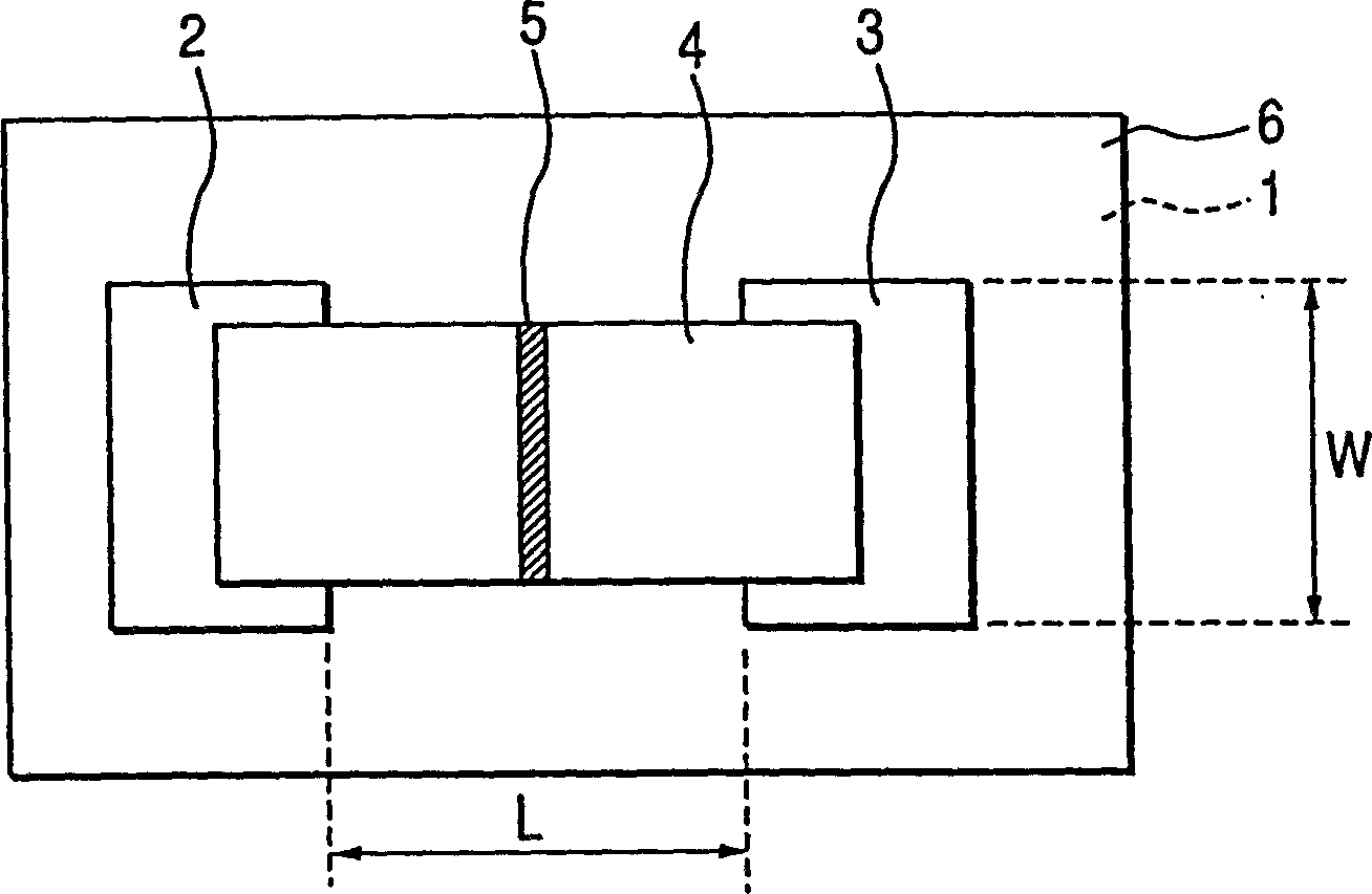
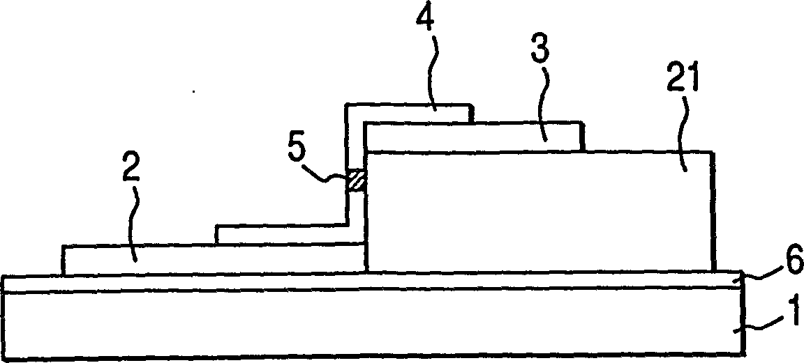
[0206] In this example, an electron source including a large number of electron-emitting devices having Figure 1A and 1B configuration, and has Figure 7 Matrix wiring setup shown. Refer below Figures 15A to 15H This fabrication process is explained for each device.
[0207] (step 1)
[0208] on SO 2 A soda lime glass substrate of the same composition as that of the substrate of Example 1 was heated at 550°C for 3 hours in a mixed flow of gas and air. Then wash with hot water and dry. The result of this step is the formation of a "de-sodiumized layer" on the surface with a thickness of about 50 μm.
[0209] (step 2)
[0210] On the "sodium-removed layer" 6 (treated surface layer) of the substrate 71, Cr and Au with a thickness of 5nm and 600nm respectively are set successively, and a photoresist (AZ1370: purchased from Hoechst Company) is formed thereon. The photomask image is then exposed and developed to produce a photoresist pattern of the lower wiring 72, and th...
Embodiment 3
[0230] In this embodiment, up to step 7 are the same as in embodiment 2, except that in step 1, a Cr thin film is formed on the periphery of the substrate by evaporation so that no "sodium-removed layer" is formed there.
[0231] Then, the shell was prepared according to step 8 in Example 2. However, in this embodiment, the electron source substrate acts as a back plate, so that no "sodium-removed layer" is formed at the junction 161 of the substrate 71 and the support frame 82. Steps 9 and 10 in Example 2 were then carried out in this example. Figure 16 The imaging device of this embodiment is schematically shown.
PUM
| Property | Measurement | Unit |
|---|---|---|
| Thickness | aaaaa | aaaaa |
| Thickness | aaaaa | aaaaa |
| Thickness | aaaaa | aaaaa |
Abstract
Description
Claims
Application Information


