Surface acoustic wave device having salient pole and its manufactruing method

A bump electrode, surface acoustic wave technology, applied in semiconductor/solid-state device manufacturing, electro-solid-state devices, piezoelectric devices/electrostrictive devices, etc., can solve the problem of reduced bonding strength, component damage, and electrical continuity failures And other issues

Inactive Publication Date: 2005-03-02
MURATA MFG CO LTD
View PDF0 Cites 0 Cited by
  • Summary
  • Abstract
  • Description
  • Claims
  • Application Information

AI Technical Summary

Problems solved by technology

As a result, a crack is caused on the piezoelectric substrate 21, which causes damage to the element, reduces the bonding strength between the element and the package 14, and causes a failure in electrical continuity.

Method used


Image

  • Surface acoustic wave device having salient pole and its manufactruing method
  • Surface acoustic wave device having salient pole and its manufactruing method
  • Surface acoustic wave device having salient pole and its manufactruing method

Examples


Embodiment Construction

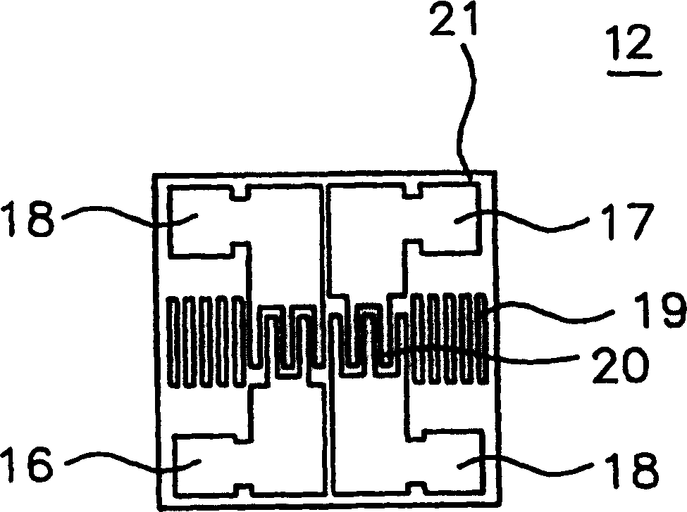
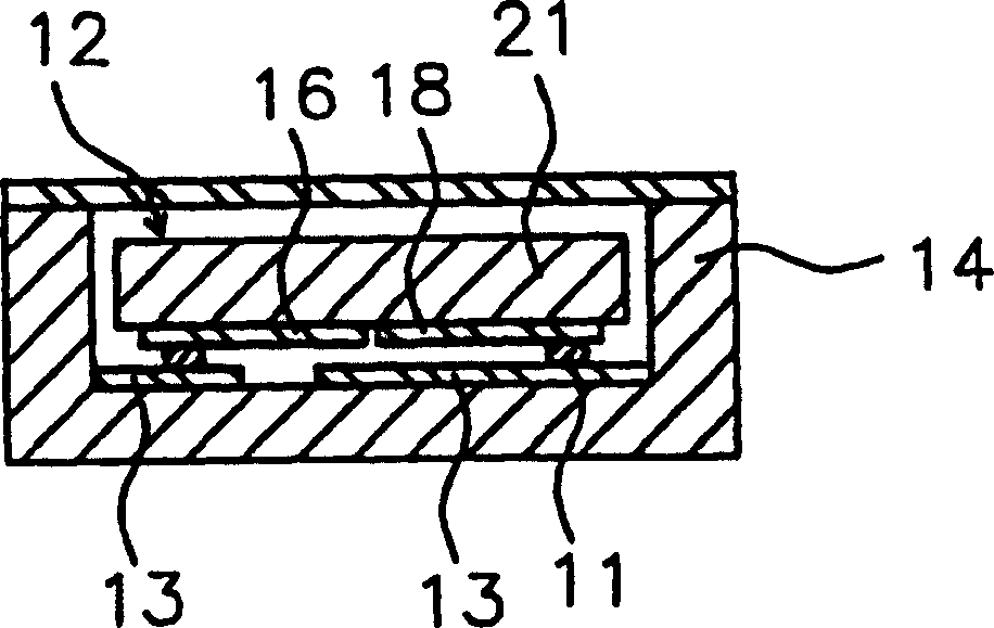
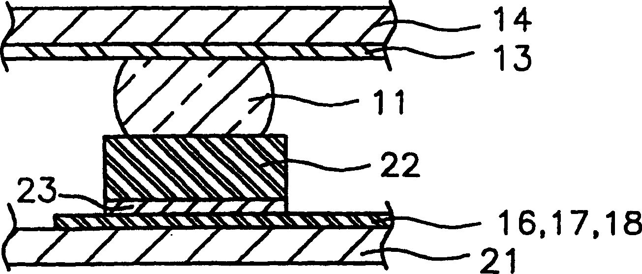
[0023] An electronic component according to a preferred embodiment of the present invention includes a substrate, an electrode pad on the substrate, an intermediate electrode provided on the electrode pad, and a bump electrode on the intermediate electrode. The electronic component also includes a base electrode disposed on the bottom of the alloy conductor. Note that the metal material of the base electrode is set and constituted so as to reduce the orientation of the intermediate electrode. By the above arrangement, the stress applied to the electrode sheet and the piezoelectric substrate during the packaging process is minimized and dissipated, so that the substrate does not crack and break.

[0024] It is preferable that the bump electrodes be made of a metal with a melting point of about 450 degrees Celsius or higher to avoid solder bumps, since heat soldering cannot be used to prevent cracking of the substrate when crimping is performed while applying ultrasonic waves or...


PUM

PropertyMeasurementUnit
melting pointaaaaaaaaaa
thicknessaaaaaaaaaa
thicknessaaaaaaaaaa

Abstract

An electronic element includes a substrate (1) with electrode pads (2) provided thereon. Intermediate electrodes (3) include base electrodes (4) on the bottom surface of the intermediate electrodes, and the bottom surface of the intermediate electrodes are disposed on the electrode pads (2). Bump electrodes (6) are provided on the intermediate electrodes (3) and include a metal having a melting point of about 450 DEG C or more. Further, the base electrodes (4) include a metallic material that can reduce orientation of the intermediate electrodes (3).

Description

technical field [0001] The present invention relates to a surface acoustic wave element with bump electrodes. In particular, the present invention relates to a surface acoustic wave element having bump electrodes that are adapted to be encapsulated to a connection portion thereof when ultrasonic waves are supplied. Background technique [0002] With the trend of miniaturization and thinning of electronic components in recent years, packaging electronic components by flip-chip bonding (in which a function of packaging a surface acoustic wave element by arranging the functional surface directly to the package surface of the substrate) has been developed surface). [0003] refer to Figure 1 to Figure 3 , describing the general structure of a surface acoustic wave device packaged by flip-chip bonding. figure 1 A plan view of the surface acoustic wave element is shown. figure 2 A cross-sectional view showing a surface acoustic wave device in which a surface acoustic wave el...

Claims


Application Information

Patent Timeline
Patent Type & Authority Patents(China)
IPC IPC(8): H01L21/60H01L41/08H02N2/00H03H3/08H03H9/05H03H9/145
CPCH03H9/059H01L2224/16225H01L2224/45144H01L2224/0508H01L2224/05568H01L2224/05023H01L2224/05001H01L2224/05124Y10T29/49144Y10T29/42Y10T29/49005Y10T29/49149H01L2924/00H01L2224/05666H01L2924/00014H01L2924/013H01L2224/05166H03H9/05H10N30/00
Inventor 田贺重人
Owner MURATA MFG CO LTD
Why Eureka
Try Eureka