

Method by using wet etching with non-equivalence in directions to carry out even process
An anisotropic, wet etching technology, applied in electrical components, semiconductor/solid-state device manufacturing, circuits, etc., to solve problems such as affecting components, surface scratches, and reduced component reliability
- Summary
- Abstract
- Description
- Claims
- Application Information
AI Technical Summary
Problems solved by technology
Method used
Image

Examples
Embodiment Construction
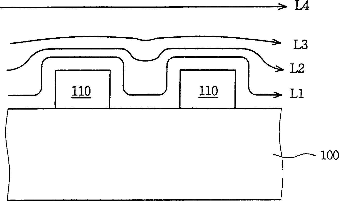
[0024] Please refer to figure 1 , figure 1 It is a schematic diagram of liquid flowing over a surface with uneven surface. There are protrusions 110 on the base 100, when the liquid flows through the surface of the base 100, according to the distance from the surface of the base 100 from near to far, in figure 1 The indicated flows are L1, L2, L3 and L4. The liquid flow L1 closest to the surface of the substrate 100 has the slowest flow velocity because it encounters the protrusion 110 on its flow path. On the contrary, the liquid flow L4 farthest from the surface of the substrate 100 has the fastest flow speed because it does not encounter any obstacles on its flowing path.
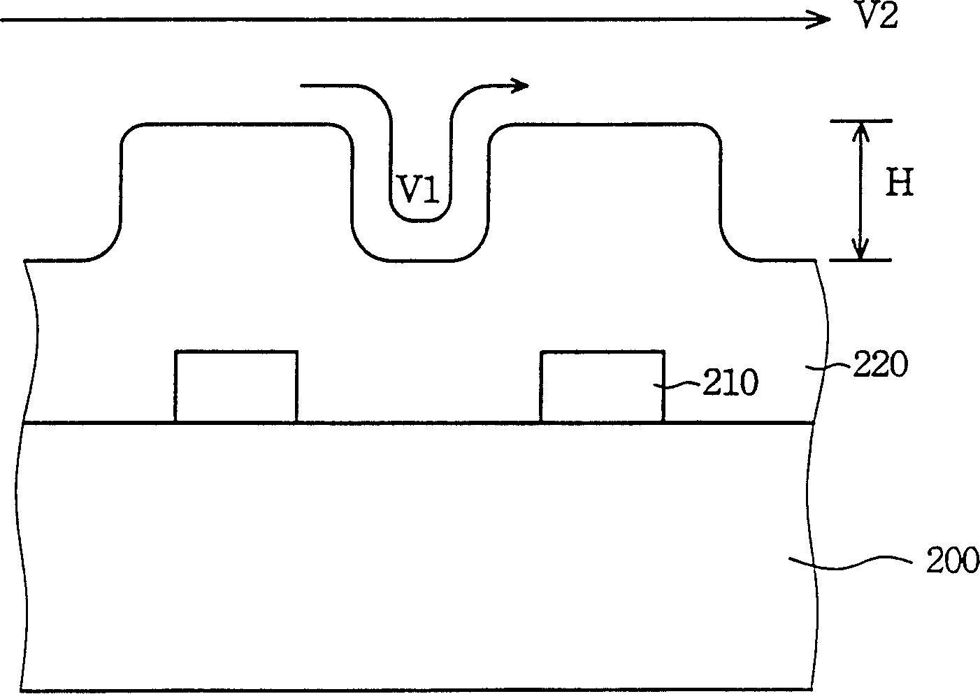
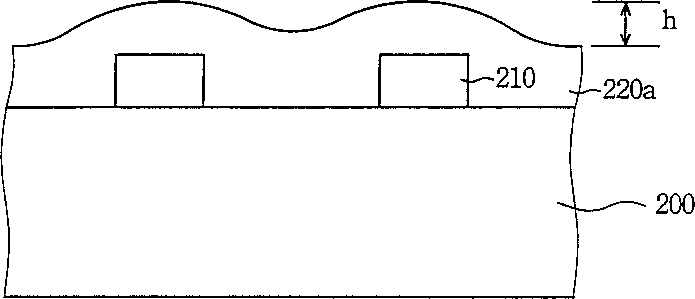
[0025] Please refer to Figure 2A-2B , which is a cross-sectional view showing a planarization process using an anisotropic wet etching method according to a preferred embodiment of the present invention. Please refer to Figure 2A , there is a wire 210 on the substrate 200, and the wire 210 can be...
PUM
 Abstract
Description
Claims
Application Information