Method for producing color filter

A technology of color filter and manufacturing method, which is applied in optics, optical components, microlithography exposure equipment, etc., and can solve problems such as unsatisfactory thickness control, incomplete shading, and impact on image quality

Inactive Publication Date: 2007-12-12
ARIMA DISPLAY
View PDF7 Cites 0 Cited by
  • Summary
  • Abstract
  • Description
  • Claims
  • Application Information

AI Technical Summary

Problems solved by technology

[0005] (1) When producing pixels of different colors, it is easy to cause overlapping or incomplete shielding between pixels of different colors of the color filter 100 due to misalignment of the manufacturing process, resulting in image distortion, and holes between pixels will also cause The interference of the interference phenomenon, so the preparation of the green pixel 1032 needs to be exposed twice, which increases the production cost; and
[0006] (2) Due to the difference in coating thickness of the blue photoresist, green photoresist and red photoresist, the surfaces of the formed blue pixel 1031, green pixel 1032 and red pixel 1033 are uneven, resulting in different colors Pixels have different photo-transmission rates, which affect image quality
[0008] However, this method of improving the planarization process is still not ideal in the thickness control of each pigment. Moreover, although the green pixel 1032 process is reduced by an exposure and development process, an etching process is added in the post process. Manufacturing process, manufacturing cost reduction is limited

Method used


Image

  • Method for producing color filter
  • Method for producing color filter
  • Method for producing color filter

Examples


Embodiment Construction

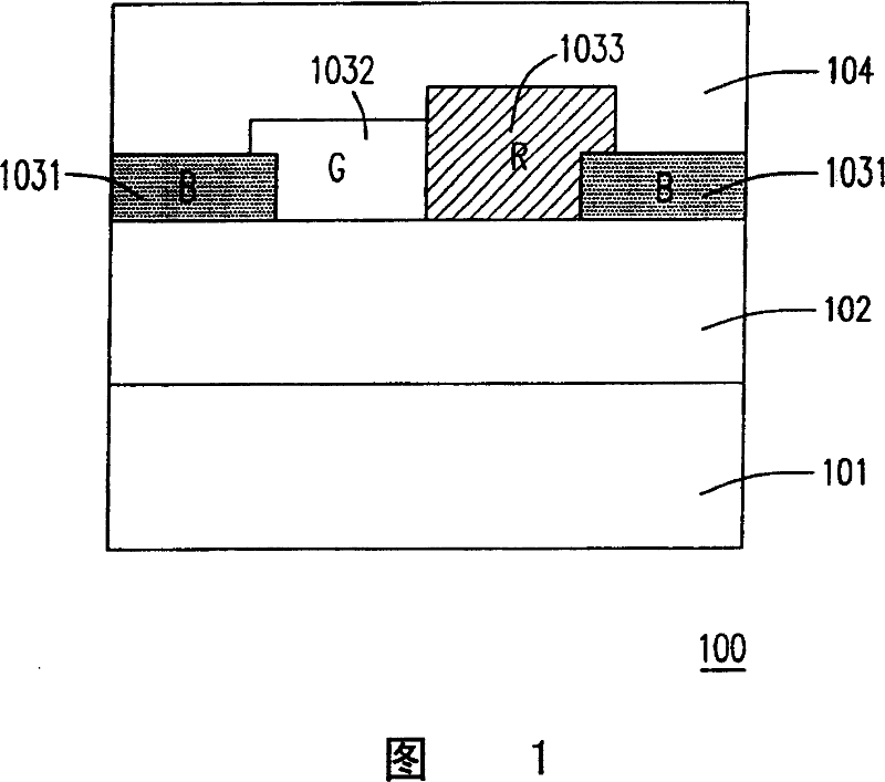
[0029] Please refer to Fig. 2 (a) to (e), which is a flow chart of a preferred embodiment of the manufacturing method of the color filter of this case.

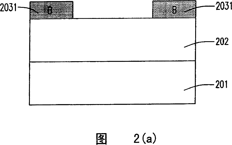
[0030] First, as shown in FIG. 2(a), a transparent and planarized dielectric layer 202 is formed on a semiconductor substrate 201, and then a color pixel with a pattern ratio of 25% is formed on the dielectric layer 202, for example Blue pixel 2031. The formation method is to coat a layer of blue photoresist on the dielectric layer 202, which is a blue dye (pigment) negative photoresist, and then perform an exposure process and a development process to harden the exposed blocks , so that the blue photoresist is transformed into many blocky blue pixels 2031, as shown in FIG. 3(a).

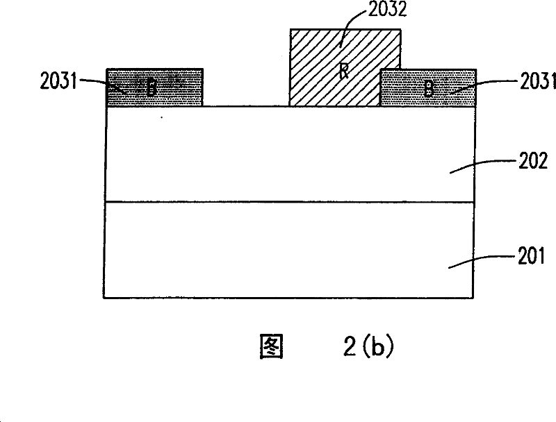
[0031] Next, as shown in FIG. 2( b ), another color pixel with a pattern ratio of 25%, such as a red pixel 2032 , is formed. The formation method is to coat a layer of red photoresist on the dielectric layer 202 and the blue pixel 2031. This red ...


PUM


Abstract

The method of producing color filter includes the following steps: providing one substrate and forming one dielectric layer on the substrate; forming the first photoresist layer and performing the first exposing and developing process to form the first pixels on the first photoresist layer; forming the second photoresist layer and performing the second exposing and developing process to make the second photoresist layer become the second pixels with superposition with the first ones in the intercrosses; forming the third photoresist layer on the dielectric layer and performing the third exposing and developing process to make the third photoresist layer cover the dielectric layer; and rolling one shaft for stretching to make the third photoresist layer become the third pixels and make the first, the second and the third pixels possess one flat surface.

Description

technical field [0001] This case refers to a method for manufacturing a color filter, especially a method for manufacturing a color filter with improved planarization technology. Background technique [0002] With the development of manufacturing technology, liquid crystal display (Liquid Crystal Display, LCD) has been a widely used display element. Whether or not liquid crystal molecules can be used to achieve a bright and dark display effect on the screen, especially for color filters used in liquid crystal panels, the quality of its manufacturing process more closely affects the performance of liquid crystal panels and the benefits they give to consumers perception. [0003] Traditionally, the procedure for making a color filter, as shown in FIG. 1 , is first to form a transparent and planarized oxide layer 102 on the semiconductor silicon substrate 101, and then cover the oxide layer 102 with a layer of blue photoresist. After one exposure and development process, the ...

Claims


Application Information

Patent Timeline
Patent Type & Authority Patents(China)
IPC IPC(8): G02B5/23G03F7/20
Inventor 陈瑞玺
Owner ARIMA DISPLAY
Why Eureka
Try Eureka