Horizontal deflection circuit and bidirectional horizontal deflection device
A technology of horizontal deflection and circuit, applied in the direction of TV, electrical components, color TV, etc., can solve the problem of forward image signal and reverse image signal offset, etc.
- Summary
- Abstract
- Description
- Claims
- Application Information
AI Technical Summary
Problems solved by technology
Method used
Image


Examples
Embodiment 1
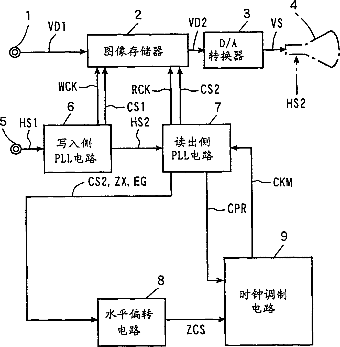
[0066] figure 1 It is a block diagram showing an example of the configuration of the bidirectional horizontal deflection device according to Embodiment 1 of the present invention.
[0067] figure 1 The bidirectional horizontal deflection device comprises input terminals 1, 5, image memory 2, D / A converter 3, write-in side phase synchronous loop (hereinafter referred to as write-in side PLL circuit) 6, read-out side phase synchronous loop (hereinafter referred to as read side PLL circuit) 7, horizontal deflection circuit 8 and clock modulation circuit 9.
[0068] The image input from the input terminal 1 is written into the image memory 2 in response to the write clock WCK given from the write-side PLL circuit 6 described later and the first switching signal CS1 indicating the switching timing of the forward scan and the reverse scan. Image data VD1. In addition, the image data VD1 stored in the image memory 2 is stored in the image memory 2 in response to the read clock R...
Embodiment 2
[0147] Fig. 8 is a circuit diagram showing the configuration of a horizontal deflection circuit of a bidirectional horizontal deflection device according to Embodiment 2 of the present invention.
[0148] The horizontal deflection circuit 8 of FIG. 8 differs from the horizontal deflection circuit 8 of FIG. 2 in that an amplitude control circuit 126 is provided instead of the amplitude control circuit 125 of FIG. 2 . The configuration of other parts of the horizontal deflection circuit 8 of FIG. 8 is the same as that of the horizontal deflection circuit 8 of FIG. figure 1 The composition of the two-way horizontal deflection device is the same. In this embodiment, the amplitude control circuit 126 corresponds to a drive timing correction circuit.
[0149] To the amplitude control circuit 126 , the correction signal VSAW and the amplitude control signal VSG that change into a sawtooth waveform at each vertical scanning period are applied. The amplitude control circuit 126 cont...
Embodiment 3
[0154] Fig. 10 is a circuit diagram showing the configuration of a horizontal deflection circuit of a bidirectional horizontal deflection device according to Embodiment 3 of the present invention.
[0155] The difference between the horizontal deflection circuit 8 of FIG. 10 and the horizontal deflection circuit 8 of FIG. 2 is that the amplitude control circuit 126 of FIG. 8 is provided on the basis of the amplitude control circuit 125 of FIG. 2 and an adder 127 is provided. The configuration of other parts of the horizontal deflection circuit 8 in FIG. 10 is the same as that of the horizontal deflection circuit 8 in FIG. figure 1 The composition of the two-way horizontal deflection device is the same.
[0156] The adder 127 adds the output signal of the amplitude control circuit 125 and the output signal of the amplitude control circuit 126 , and applies an output signal indicating the addition result to the other input terminal of the adders 107 and 108 .
[0157] By addin...
PUM
 Abstract
Description
Claims
Application Information