Method for making three-dimension microstructure and

A manufacturing method and microstructure technology, which are applied in the photo-engraving process, optics, opto-mechanical equipment and other directions of the pattern surface, can solve the problem that the continuous surface cannot be used to form shapes, etc., so as to improve the production efficiency, reduce the production cost, and save the plate making. The effect of craftsmanship

Inactive Publication Date: 2005-10-19
INST OF OPTICS & ELECTRONICS - CHINESE ACAD OF SCI
View PDF0 Cites 0 Cited by
  • Summary
  • Abstract
  • Description
  • Claims
  • Application Information

AI Technical Summary

Problems solved by technology

However, this method requires the microstructure to be fabricated to be symmetric and cannot be used for forming continuous surface shapes, so it has certain limitations.

Method used


Image

  • Method for making three-dimension microstructure and
  • Method for making three-dimension microstructure and
  • Method for making three-dimension microstructure and

Examples


Embodiment Construction

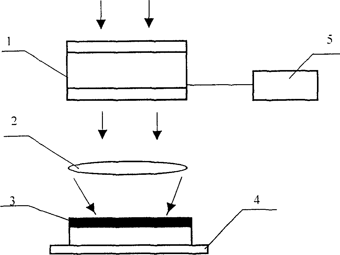
[0030] Such as figure 1 As shown, the exposure device used in the embodiment of the present invention includes a projection exposure lens 2 , an exposure table 4 and a computer 5 . An electrically addressable (or optically addressable) liquid crystal light valve 1 as a real-time mask is placed above the projection exposure lens 2 . The switch of each light-passing unit of the electrical addressing (or optical addressing) liquid crystal light valve 1 is programmed and controlled by the computer 5, which acts as a mask. Each light-passing unit of the liquid crystal light valve 1 corresponds to a sampling point of the mask pattern. Since the switching status of each light-passing unit of the liquid crystal light valve 1 can be continuously refreshed as required, it is called a real-time mask. The projection exposure lens 2 is placed under the liquid crystal light valve 1 . The real-time mask pattern passes through the light-passing unit of the liquid crystal light valve 1 , an...


PUM


Abstract

The invention discloses a manufacturing method of three-deimensional micro-structure and exposal device it used. This method uses masking graph engendered by computer to expose the sensitive material repeatedly, then, it moves the exposal platform and exposes various area of sensitive material; in the end, it develops and forms random successive three-dimensional micro-structure. Exposal device used in this method includes computer, liquid crystal light valve, projection lens and exposal platform. The invention can make micro-structure component which has a large general area, avoids oif expensive and time consuming plate-making craft, reduces the manufacturing cost of micro-structure and further enhances the manufacturing efficiency and precision.

Description

technical field [0001] The invention relates to a manufacturing method of a three-dimensional microstructure. Background technique [0002] In recent years, with the rise of micro-optomechanical and micro-opto-electromechanical systems, a variety of fabrication techniques for three-dimensional microstructures have been developed. The existing three-dimensional microstructure microfabrication technology originates from the large-scale integrated circuit manufacturing process, and the most representative ones are as follows: [0003] "Optical Engineering" published in 1978, Volume 17, pages 570-573 "The past, present and future of diamond optical milling" discloses a single-point diamond milling method (references: "Dimond turning of optics: the past, the presaent, and the exciting future", Opt. Eng, 1978, Vol.17: 570-573). The components produced by this method have high scoring precision, but the milling residues have large particle size (greater than 10 microns), which is...

Claims


Application Information

Patent Timeline
Patent Type & Authority Patents(China)
IPC IPC(8): G02B27/22G03F7/22
Inventor 曾红军陈波杜春雷郭履容
Owner INST OF OPTICS & ELECTRONICS - CHINESE ACAD OF SCI
Why Eureka
Try Eureka