
Method for producing metal layer virtual pattern

A technology of virtual patterns and metal layers, which is applied in the fields of electrical components, semiconductor/solid-state device manufacturing, circuits, etc., and can solve problems such as metal wiring load effects

Inactive Publication Date: 2005-12-14
WINBOND ELECTRONICS CORP
View PDF0 Cites 0 Cited by
  • Summary
  • Abstract
  • Description
  • Claims
  • Application Information

AI Technical Summary

Problems solved by technology

[0008] Therefore, the object of the present invention is to provide a method for generating a metal layer pattern, which can solve the known problem of loading effect when making metal wiring.

Method used


Image

  • Method for producing metal layer virtual pattern
  • Method for producing metal layer virtual pattern
  • Method for producing metal layer virtual pattern

Examples


no. 1 example

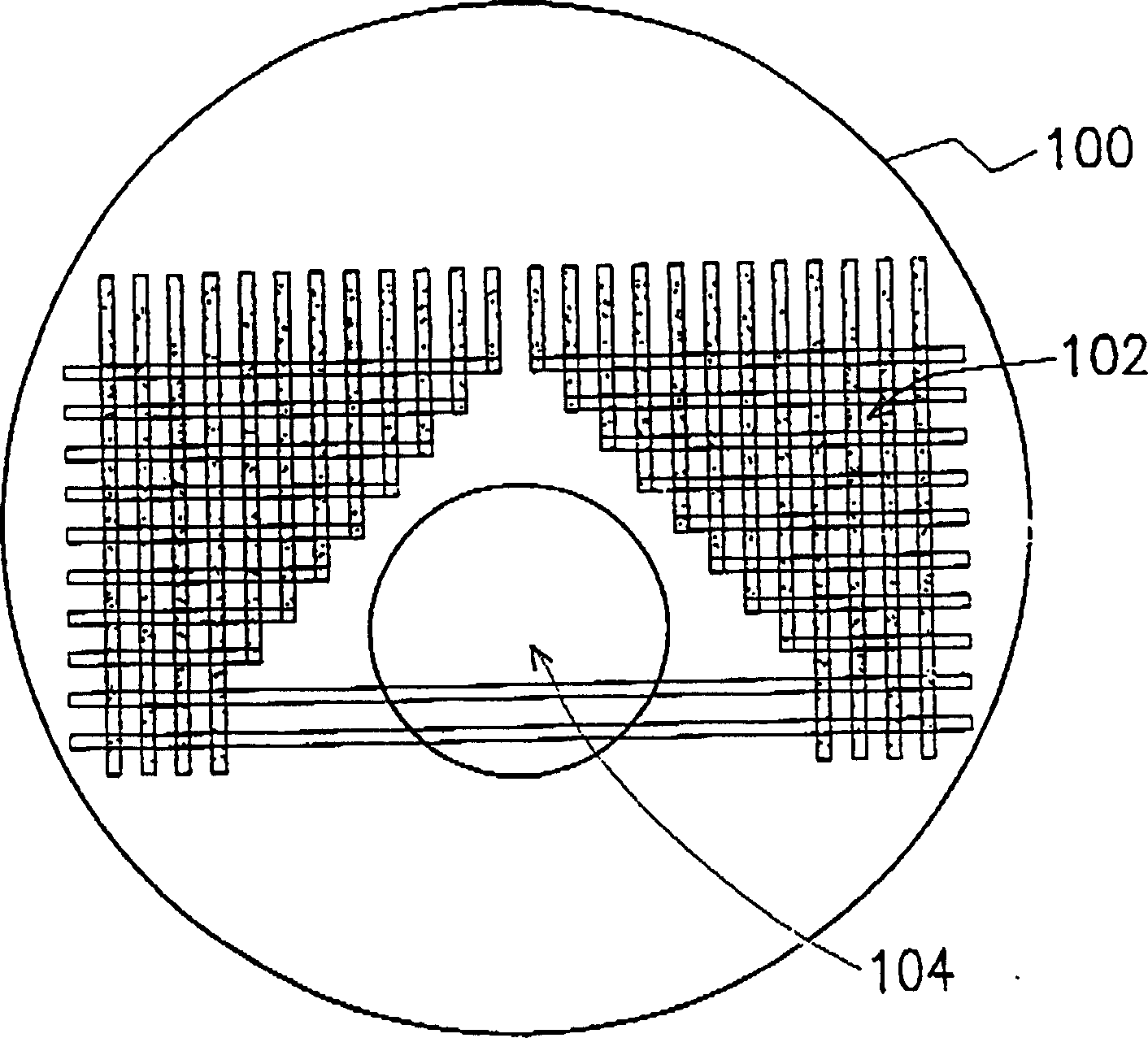
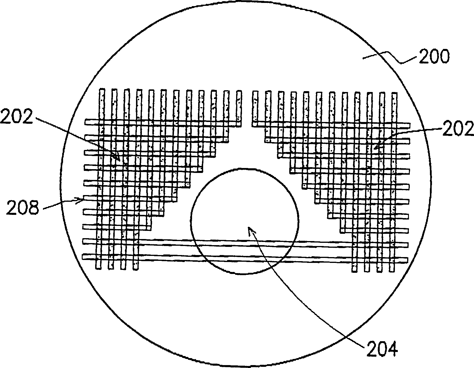
[0030] Figure 2A 2B is a schematic diagram of a design method with a metal layer dummy pattern according to a first preferred embodiment of the present invention, Figure 2A 2B is a top view of a silicon chip.

[0031] Please refer to Figure 2A Firstly, a semiconductor substrate 200 is provided. The substrate 200 includes a metal layer pattern dense area 202 and a metal layer pattern sparse area 204 . The metal layer pattern density of the metal layer pattern dense area 202 is higher than that of the metal layer pattern sparse area 204 . The metal layer pattern of the metal layer pattern dense area 202 includes, for example, a first metal layer pattern 206 with a first direction and uniform pattern density on the bottom layer, and a second metal layer pattern 206 with a uniform pattern density on the upper layer. The metal layer pattern 208, wherein the first direction is perpendicular to the second direction. In addition, the metal layer pattern in the metal layer patter...

no. 2 example

[0039] Figure 3A to Figure 3G A cross-sectional view of a process for generating a dummy pattern of a metal layer according to a second preferred embodiment of the present invention, wherein Figure 3F to Figure 3G The flow chart is presented in a top perspective view, Figure 3E for Figure 3F Section along the I-I tangent.

[0040] Please refer to Figure 3AA semiconductor silicon substrate 300 is provided, and a dielectric layer 302 and a metal layer 304 are sequentially formed on the substrate 300 . The material of the metal layer 304 is, for example, aluminum, copper, aluminum-copper alloy, or any other metal.

[0041] Please refer to Figure 3B The metal layer 304 is defined by typical photolithography and etching methods to form a plurality of metal lines 304a with a first direction, wherein the metal lines 304a have a uniform pattern density.

[0042] Next, according to the metal interconnection pattern to be formed, the connection between some unnecessary metal...


PUM


Abstract

A method for generating a dummy metal layer pattern, which is to provide a dummy metal layer pattern on an original chip with a fixed layout when making metal wiring, so that the density of the pattern everywhere on the chip is uniform, avoiding the known and common The problem of load effect is beneficial to the follow-up process, so as to improve the reliability of components and increase the yield of production.

Description

technical field [0001] The present invention relates to a method for forming a semiconductor device, and more particularly to a method for generating a dummy pattern of a metal layer when performing metal interconnect. Background technique [0002] With the improvement of integration in integrated circuits, the design of interconnects with more than two layers has gradually become a necessary method for many integrated circuits. Usually, the dry etching process using plasma is quite suitable for the manufacture of high-density semiconductor components. Therefore, the dry etching process is more and more important for the manufacture of high-density semiconductor components. Dry etching process is also often used to etch the metal layer to form the desired metal interconnect pattern. [0003] In order to define the pattern of the circuit on the silicon chip, a typical method is to use a photolithography process to transfer the circuit layout pattern on the silicon chip. Nex...

Claims


Application Information

Patent Timeline
IPC IPC(8): H01L21/768
Inventor 叶垂奇张威彦
Owner WINBOND ELECTRONICS CORP
Learn More