Pixel structure and mfg method therefor

A technology of pixel structure and manufacturing method, applied in static indicators and other directions, can solve the problems of load effect, different key dimensions, etc.

Active Publication Date: 2005-12-21
AU OPTRONICS CORP
View PDF0 Cites 11 Cited by
  • Summary
  • Abstract
  • Description
  • Claims
  • Application Information

AI Technical Summary

Problems solved by technology

[0007] In view of this, the object of the present invention is to provide a pixel structure and its manufacturing method, which can solve the problem of loading effect caused by different key dimensions, and achieve better control of device characteristics

Method used


Image

  • Pixel structure and mfg method therefor
  • Pixel structure and mfg method therefor
  • Pixel structure and mfg method therefor

Examples


no. 1 example

[0040] The following is a method for manufacturing a pixel structure according to the first embodiment of the present invention.

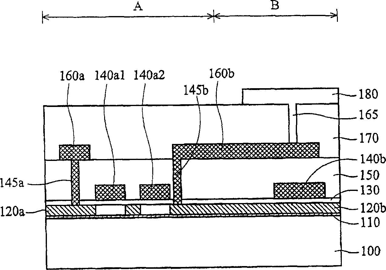
[0041] Figure 3A In order to show a cross-sectional schematic diagram of a patterned semiconductor layer formed on a substrate according to an embodiment of the present invention, it includes a thin film transistor (TFT) area A and a capacitor area B. First, the buffer layer 310 can be formed on the substrate 300 by means of chemical vapor deposition (CVD) or the like. The substrate 300 may include materials such as glass, and the buffer layer 310 may include materials such as silicon oxide and / or silicon nitride.

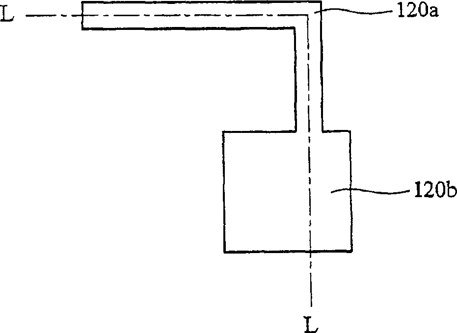
[0042] Next, a semiconductor layer is deposited on the buffer layer 310, and then a photolithography etching process is performed to form the active layer 320a, the bottom electrode 320b, and the opening 320c. The active layer 320a and the lower electrode 320b are not connected, and the opening 320c is used as the interval. The top view i...

no. 2 example

[0049] Figure 5A In order to show a cross-sectional schematic diagram of a patterned semiconductor layer formed on a substrate according to an embodiment of the present invention, it includes a thin film transistor (TFT) area A and a capacitor area B. First, the buffer layer 510 is formed on the substrate 500 by, for example, chemical vapor deposition (CVD) or the like. The substrate 500 may include materials such as glass, and the buffer layer 510 may include materials such as silicon oxide and / or silicon nitride.

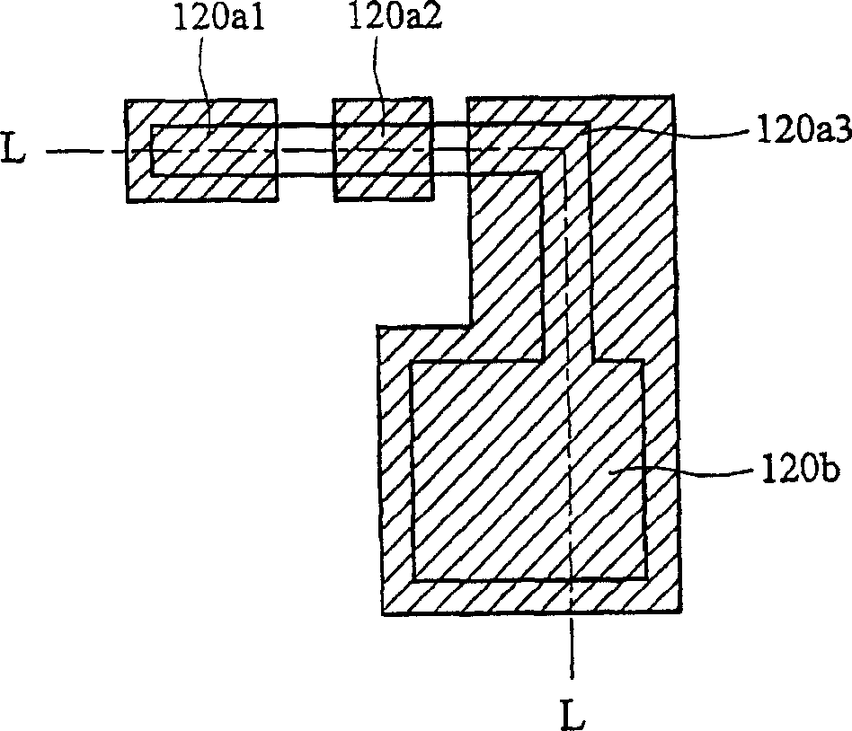
[0050] Next, a semiconductor layer is deposited on the buffer layer 510, and then a photolithography etching process is performed to simultaneously form the active layer 520a, the bottom electrode 520b, and the opening 520c. The active layer 520a and the lower electrode 520b are not connected, and the opening 520c is used as the interval. The top view is as Figure 6A Shown along Figure 6A The section view of the middle section line L’L’ is Figure 5A . This struct...


PUM


Abstract

The pixel structure includes thin film transistor formed on basal plate, and storage capacitance. The thin film transistor possesses grid electrode and active layer. The active layer includes at least source electrode region and drain electrode region. First adulterant is adulterated on source electrode region and drain electrode region. Formed on the basal plate, the storage capacitance possesses lower electrode and upper electrode. Second adulterant is adulterated on the lower electrode. First adulterant is differed from second adulterant in type. The source electrode region and drain electrode region are not connected to the lower electrode.

Description

Technical field [0001] The present invention relates to a pixel structure, in particular to a pixel structure in which a source region and a drain region are not connected to a lower electrode, and a manufacturing method thereof. Background technique [0002] Liquid crystal display (LCD) is one of the most common displays at present. Thin Film Transistor (TFT) is often used as its active element to control the rotation of liquid crystal, and capacitors are used for storage. Charge to maintain the picture. [0003] figure 1 It is an existing pixel structure diagram, including a thin film transistor area A and a capacitor area B. The two areas include a substrate 100, a buffer layer 110, an active layer 120a and a lower electrode layer 120b of the capacitor, a dielectric layer 130, and a gate electrode 140a1. , 140a2 and the upper electrode 140b, the insulating layer 150, the signal line 160a and the second metal layer 160b. The signal line 160a is in contact with the source elec...

Claims


Application Information

Patent Timeline
Patent Type & Authority Applications(China)
IPC IPC(8): G02F1/133
Inventor 刘圣超尤建盛李春生
Owner AU OPTRONICS CORP
Why Eureka
Try Eureka