Semiconductor luminous device

A technology of light-emitting devices and semiconductors, which is applied to semiconductor devices, semiconductor lasers, laser components, etc., and can solve problems such as low response speed and reduced device response speed

Inactive Publication Date: 2006-03-29
SHARP KK
View PDF3 Cites 0 Cited by
  • Summary
  • Abstract
  • Description
  • Claims
  • Application Information

AI Technical Summary

Problems solved by technology

This low current density region has a low response speed, resulting in a problem that the response speed of the entire device decreases

Method used


Image

  • Semiconductor luminous device
  • Semiconductor luminous device
  • Semiconductor luminous device

Examples


Embodiment Construction

[0049] The present invention will be described in detail below in conjunction with embodiments and with reference to the accompanying drawings.

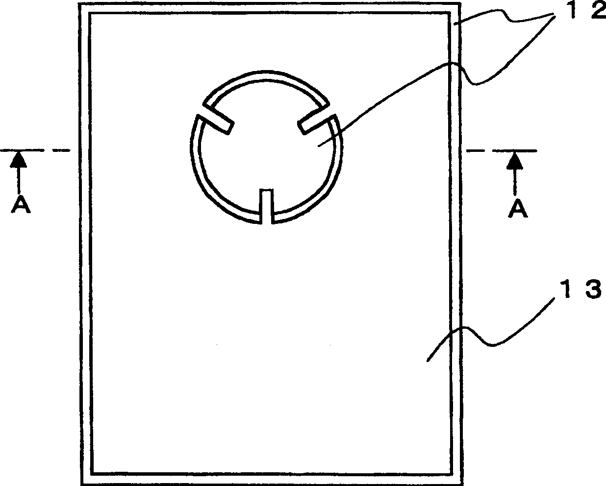
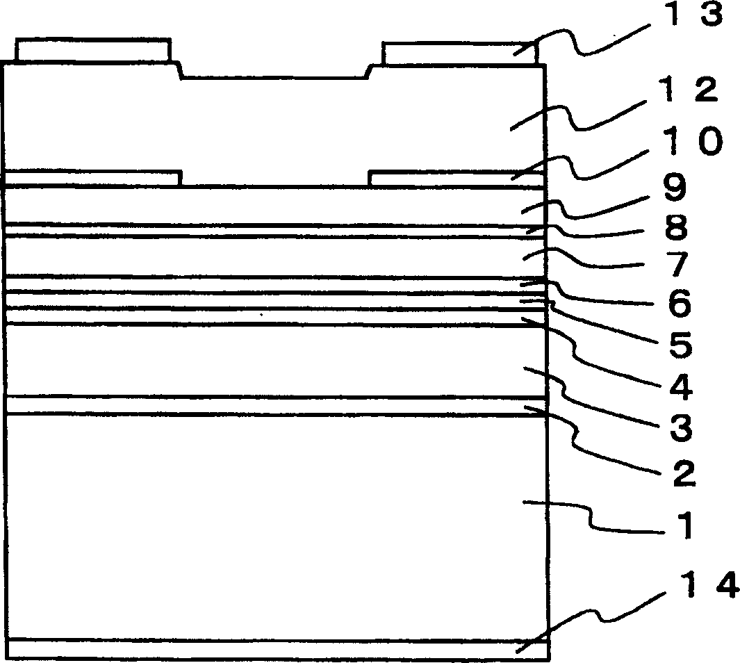
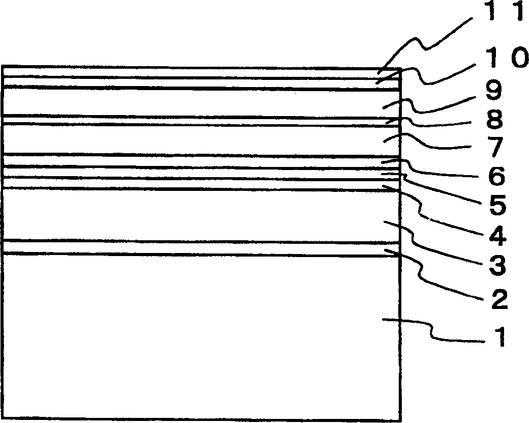
[0050] Figure 1A is a plan view of the semiconductor light emitting device in the first embodiment of the present invention. Figure 1B for along Figure 1A Sectional view taken along line A-A of . figure 2 for the manufacturing process, showing Figure 1A with 1B A cross-sectional view of the state of the semiconductor light-emitting device shown. Figure 3A In order to show the difference of semiconductor light-emitting devices in the manufacturing process figure 2 State floor plan. Figure 3B for along Figure 3A Sectional view taken along line B-B of .

[0051] The semiconductor light emitting device of this embodiment is an AlGaInP-based semiconductor light emitting device. First, on an n-type GaAs substrate 1 which is a semiconductor substrate inclined at 15° in the [011] direction from the (100) plane, as figure 2 A...


PUM


Abstract

A resonant cavity type light emitting diode has a first DBR made of n-type AlAs or Al0.5Ga0.5As, a quantum well active layer, a second DBR made of p-type (Al0.2Ga0.8)0.5In0.5P or Al0.5In0.5P, and an n-type current constriction layer on an n-type GaAs substrate. The first DBR and the second DBR form a resonator. The quantum well active layer is formed in a position of an antinode of a standing wave inside the resonator. Between the second DBR and the current constriction layer, there is provided a p-type GaP etching protection layer that has a value obtained by dividing resistivity by thickness being 1x10<3 >Omega or more. Since a current in a current flow pass formed in the current constriction layer hardly diffuses to the outside of the current flow pass, there is generated few region with low current density that causes deterioration of response speed in a quantum well layer. Thus, the light emitting diode has an excellent high-speed response.

Description

technical field [0001] The present invention relates to semiconductor light emitting devices. Background technique [0002] In recent years, semiconductor light-emitting devices have been widely used in information display panels, optical communications and other fields. These semiconductor light emitting devices not only need to have high light emission efficiency, but also need to have high-speed response, especially when they are applied in the field of optical communication. Therefore, fast semiconductor light emitting devices with higher efficiency and faster response have been vigorously developed. [0003] Surface-emitting LEDs (light-emitting diodes), which allow low operating currents, have attracted attention as a high-efficiency semiconductor light-emitting device. However, surface-emitting LEDs are relatively insufficient in terms of high-speed response. The data transmission speed of surface-emitting LEDs is best at about 100Mbps to 200Mbps. As a result, res...

Claims


Application Information

Patent Timeline
Patent Type & Authority Patents(China)
IPC IPC(8): H01L33/00H01S5/183H01S5/343H01L33/06H01L33/14H01L33/30
CPCH01L33/105
Inventor 仓桥孝尚村上哲朗大山尚一中津弘志
Owner SHARP KK
Why Eureka
Try Eureka