Wavelength division multiplex optical switch

a multi-wavelength, optical switch technology, applied in the field of optical switches, can solve the problems of reducing switching speed, increasing power consumption of photoelectric transducers and electro-optic transducers, and difficult to cope with the larger capacity and higher-speed of a future optical communication system, and achieve excellent high-speed response and consumption. less power

Inactive Publication Date: 2005-08-09
HITACHI LTD
View PDF11 Cites 2 Cited by
  • Summary
  • Abstract
  • Description
  • Claims
  • Application Information

AI Technical Summary

Benefits of technology

[0008]The invention has been made in view of the foregoing, and provides an optical switch that consumes less power, is excellent in a high-speed response, and possesses a structure suitable for a miniaturization and multi-channel switching.

Problems solved by technology

As the number of the relay points increases, the total power consumption of the photoelectric transducers and electro-optic transducers increases, and the switching speed decreases.
However, since the switching time of the conventional optical switch takes some millisecond, it is difficult to cope with the larger capacity and higher-speed for a future optical communication system.
Also, the conventional optical switching system requires a high electric driving force for switching, and needs still higher energy consumption.
Therefore, it is difficult to miniaturize the optical switch for multi-channel switching.
In addition, since the variation range of the refractive index is extremely small, the laser power for inducing the variation of about 2% of the refractive index is as high as about 5 to 50 MW / cm2, and the power consumption of the total device increases.

Method used


Image

  • Wavelength division multiplex optical switch
  • Wavelength division multiplex optical switch
  • Wavelength division multiplex optical switch

Examples


embodiment 1

[Embodiment 1]

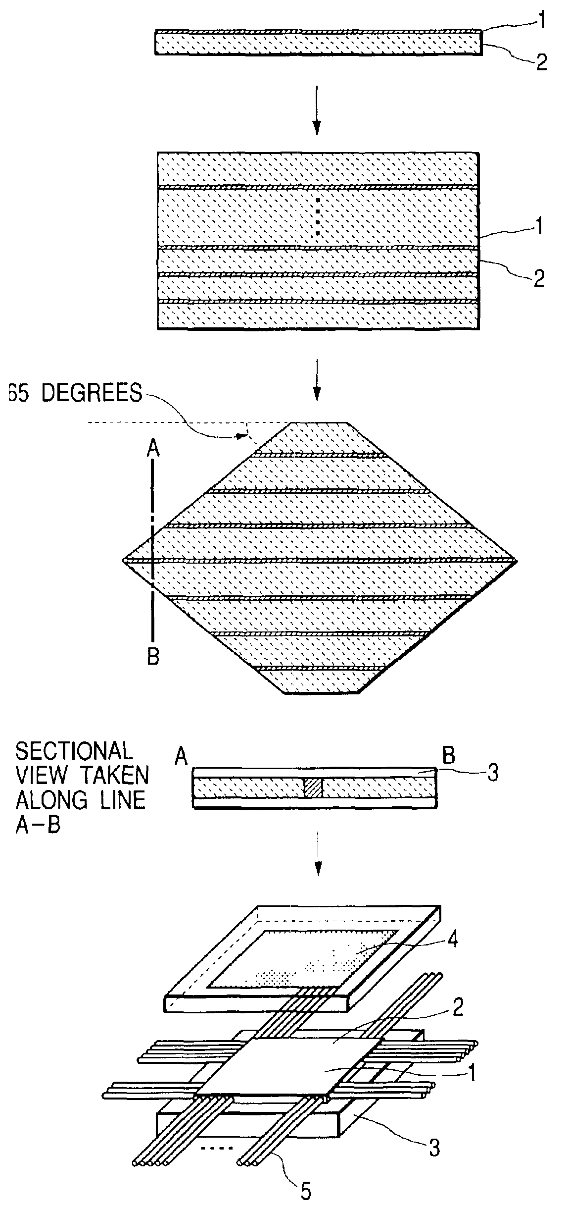
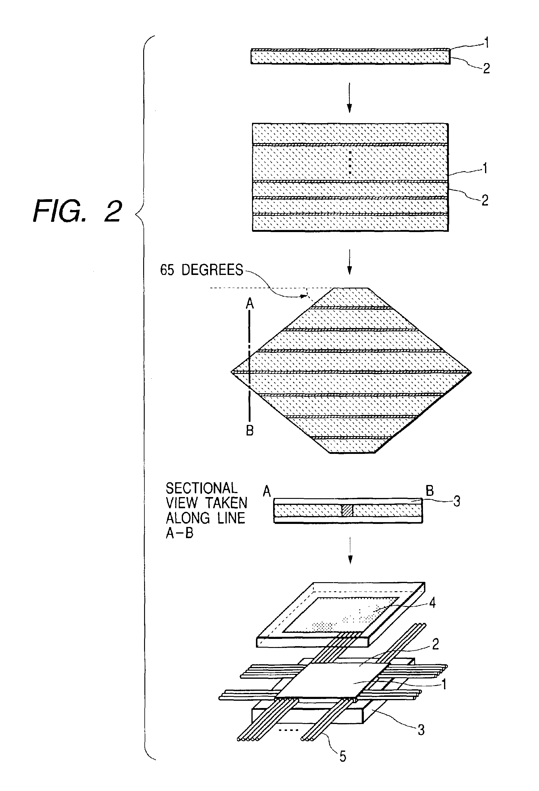
[0021]Preferred embodiments of an optical switch according to the invention will be described with reference to FIG. 1 through FIG. 11.

[0022]FIG. 1 is a perspective view illustrating the structure of a multi-channel optical switch. The multi-channel optical switch of a first embodiment includes a laminated structure in which buffer layers or substrates 1 and nonlinear optical layers or nonlinear optical films 2 are alternately laminated in 16 layers, a supporting substrate 3, and a surface emitting laser 4.

[0023]The surface emitting laser 4 may be disposed on any one between the laminated structure and the supporting substrate, or it may be disposed between both sides of the laminated structure and each of the supporting substrate. The positions of the emitting points inside the surface-emitting laser may be arranged regularly or irregularly. In the case where the surface emitting lasers are provided on both sides of the laminated structure, the emitting positions may ...

embodiment 2

[Embodiment 2]

[0055]In a second embodiment as illustrated in FIG. 11, a Cr electrode is mounted on the upper side of a part to be excited, and under a supporting substrate, a Cr electrode is formed on the whole surface of a lower substrate as a lower electrode. In other words, an electrode 8 is mounted on the outside of the substrate 3.

[0056]The second embodiment 2 has a construction for using an electric field, in contrast to the embodiment 1 that uses the laser beams (excited light) as the external field.

[0057]It was observed that when a voltage of 40 volts was applied to the nonlinear optical thin film 2 through a Cr electrode 8 and a lower metal film, an optical path of outgoing light changed from core b to core c in the same manner as the first embodiment 1 involving irradiation with the excited light 10.

[0058]However, it was found that a response to the applied pulse voltage was 1000 nanosecond order, which is slow in comparison to the first embodiment. The second embodiment p...

embodiment 3

[Embodiment 3]

[0059]An experiment was made such that a fluorescence film ZnS was made luminous by voltage, and the luminescence created a refractive index variation in a nonlinear optical thin film.

[0060]A device structure such that the electrode 8 in FIG. 11 is changed into a luminescent surface is used. ZnS and Cr electrodes are deposited on the supporting substrate attached on the uppermost surface. When 40 volts are applied across the Cr electrodes, the ZnS thin film emits fluorescence.

[0061]Using this fluorescence gave a variation of the refractive index in the nonlinear optical thin film 2, which confirmed a switching phenomenon with the same speed as that of the embodiment 2. This result found that the fluorescence caused by applying an electric field effected the switching.

[0062]According to the invention, a small matrix optical switch excellent in a high-speed response and suitable for switching a large-capacity of information can be achieved by providing a laminated struct...


PUM

PropertyMeasurementUnit
angleaaaaaaaaaa
particle diameteraaaaaaaaaa
thickaaaaaaaaaa

Abstract

The invention provides an optical switch that consumes a less power, excels in a high-speed response, and possesses a structure suitable for a miniaturization and multi-channel switching. The optical switch switches a plurality of input signals to a plurality of output positions, in which a laminated structure that has a nonlinear optical layer and a buffer layer laminated in the same number as that of input parts intersects an optical path between the input parts and output parts. By providing the laminated structure using the nonlinear optical thin films, the invention achieves a small matrix optical switch excellent in a high-speed response and suitable for switching a large-capacity of information.

Description

BACKGROUND OF THE INVENTION[0001]The present invention relates to an optical switch, and specifically to an optical switch that controls the output of inputted light.[0002]A further development of the information-oriented society involves building up an optical communication system that implements a high-speed transmission of a large-capacity of information. At present, the wavelength division multiplex (WDM) communication system has been developed, further accelerating the transmission speed of a network.[0003]One of devices essential for a still faster optical communication system is a switching means of optical information. The conventional switching system of optical information required, at each relay point, a photoelectric transducer that converts optical information into electric information once and an electro-optic transducer that converts the electric information reversely into the optical information.[0004]As the number of the relay points increases, the total power consu...

Claims


Application Information

Patent Timeline
Patent Type & Authority Patents(United States)
IPC IPC(8): G02F1/35G02B6/35G02F1/315
CPCG02F1/3515G02B6/3512G02B6/3546G02F1/35
Inventor HONDA, MITSUTOSHISAWAI, YUICHIISHIKAWA, TAKAONAITO, TAKASHI
Owner HITACHI LTD
Why Eureka
Try Eureka