Grid structure and manufacture method as well as MOS part of grid structure

A gate structure and manufacturing method technology, applied in the field of metal oxide semiconductor transistors and their manufacturing, can solve the problems of reduced electrical characteristics of transistors, longer electron travel paths, and reduced element operation speed.

Inactive Publication Date: 2006-07-05
TAIWAN SEMICON MFG CO LTD
View PDF0 Cites 0 Cited by
  • Summary
  • Abstract
  • Description
  • Claims
  • Application Information

AI Technical Summary

Problems solved by technology

When a voltage is subsequently applied to the gate 104a to allow electrons to reach the drain from the source through the channel below the gate 104a, the uneven electric field caused by the uneven interface between the gate 104a and the semiconductor substrate 101 will make the electrons in the channel The electrons are affected, causing the electrons to travel a longer path and degrading the electrical characteristics of the transistor
[0008] At the same time, in order to increase the density of components, the size of the components will be reduced as much as possible to increase the number of components; however, when the size of the components is reduced, the poly gate depletion effect (PED) will become serious
The so-called polysilicon gate depletion effect is that when the size of the device is reduced, the ratio of the depletion region between the metal layer and the oxide layer will increase and affect the speed of electrons, so that the operating speed of the device will be reduced

Method used


Image

  • Grid structure and manufacture method as well as MOS part of grid structure
  • Grid structure and manufacture method as well as MOS part of grid structure
  • Grid structure and manufacture method as well as MOS part of grid structure

Examples


Embodiment Construction

[0018] Figure 2a-2f Shown is a schematic flow chart of the steps of manufacturing the grid of the present invention.

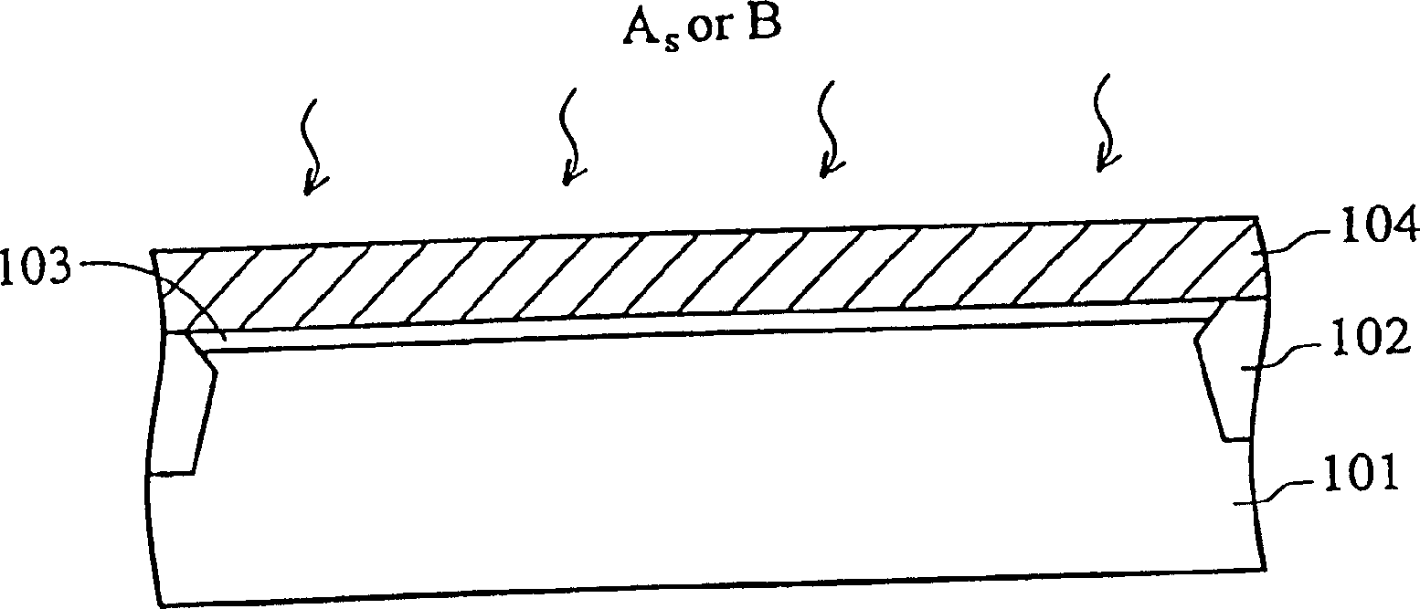
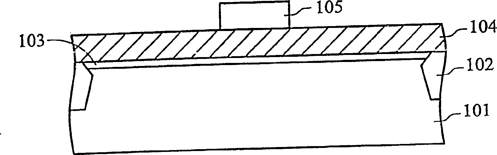
[0019] Please refer to Figure 2a Firstly, a semiconductor substrate 201 is provided, the semiconductor substrate 201 has an isolation region 202 , and the isolation region 202 is used to isolate an active region on the semiconductor substrate 201 . An oxide layer 203 is formed in the active region on the semiconductor substrate 201, and with hydrogen (H 2 ) and silane (SiH 4 ) in a processing chamber to perform a deposition step on the semiconductor substrate 201 . Wherein, the isolation region 202 can be a shallow trench isolation layer; the oxide layer 203 can be silicon dioxide, which is used as a gate oxide layer.

[0020] Please refer to Figure 2b , with hydrogen (H 2 ) and silane (SiH 4 ) after the semiconductor substrate 201 is deposited in the processing chamber, a first polysilicon and amorphous silicon mixed layer 204 will be formed on the ...


PUM


Abstract

The grid structure includes first part of polysilicon layer as bottom layer, a polysilicon layer, and second partial polysilicon layer as top layer. The MOS semiconductor includes semiconductor substrate, a grid oxide layer forming on the semiconductor substrate, and a multi layer structural grid electrode including a polysilicon layer as bottom layer, a polysilicon middle layer and part of polysilicon top layer. Depositing semiconductor substrate under hydrogen environment forms the said first part of polysilicon layer and second part of polysilicon layer. The invention can manufacture transistors having following advantages: high grid activity of polysilicon, smooth surface of partial polysilicon, low cavity effect of polysilicon grid electrode and high carrier activity.

Description

technical field [0001] The invention relates to a transistor and a manufacturing method thereof, in particular to a metal oxide semiconductor transistor and a manufacturing method thereof. Background technique [0002] Metal-Oxide-Semiconductor Transistor (MOS) is a very important basic electronic component in VLSI technology. It is mainly composed of three basic materials, namely metal conductor layer, oxide layer and semiconductor layer. The gate transistor on the substrate; in addition, it also includes two semiconductor regions located on both sides of the gate transistor and electrically opposite to the semiconductor substrate, called source and drain. At present, when manufacturing gate transistors, the metal conductive layer is mostly composed of doped polysilicon (Polysilicon) and metal, and this structure is also called polycide. [0003] Figure 1a-1c Shown is a flow chart of known steps for fabricating a gate. [0004] Please refer to Figure 1a Firstly, a semi...

Claims


Application Information

Patent Timeline
Patent Type & Authority Patents(China)
IPC IPC(8): H01L29/78H01L21/28H01L21/336
Inventor 陈佳麟姚亮吉陈世昌
Owner TAIWAN SEMICON MFG CO LTD
Why Eureka
Try Eureka