
Circuit structure for connecting weld-pad and electrostatic protective circuit

A technology of electrostatic discharge protection and circuit structure, applied in circuits, electrical components, electrical solid devices, etc., can solve the problems of unfavorable component integration, reduced process margin, etc., achieve large variability and freedom, enhance protection ability, Avoid the effect of failure

Inactive Publication Date: 2006-11-22
UNITED MICROELECTRONICS CORP
View PDF0 Cites 0 Cited by
  • Summary
  • Abstract
  • Description
  • Claims
  • Application Information

AI Technical Summary

Problems solved by technology

However, if the thickness W of the extension wire 112a is limited, the extension wire 112a can only solve the problem by widening the wire.
In today's technology where semiconductor components are becoming smaller and more highly integrated, the increase in line width means the reduction of the process margin (window), which is not conducive to the integration of components.

Method used


Image

  • Circuit structure for connecting weld-pad and electrostatic protective circuit
  • Circuit structure for connecting weld-pad and electrostatic protective circuit
  • Circuit structure for connecting weld-pad and electrostatic protective circuit

Examples


Embodiment Construction

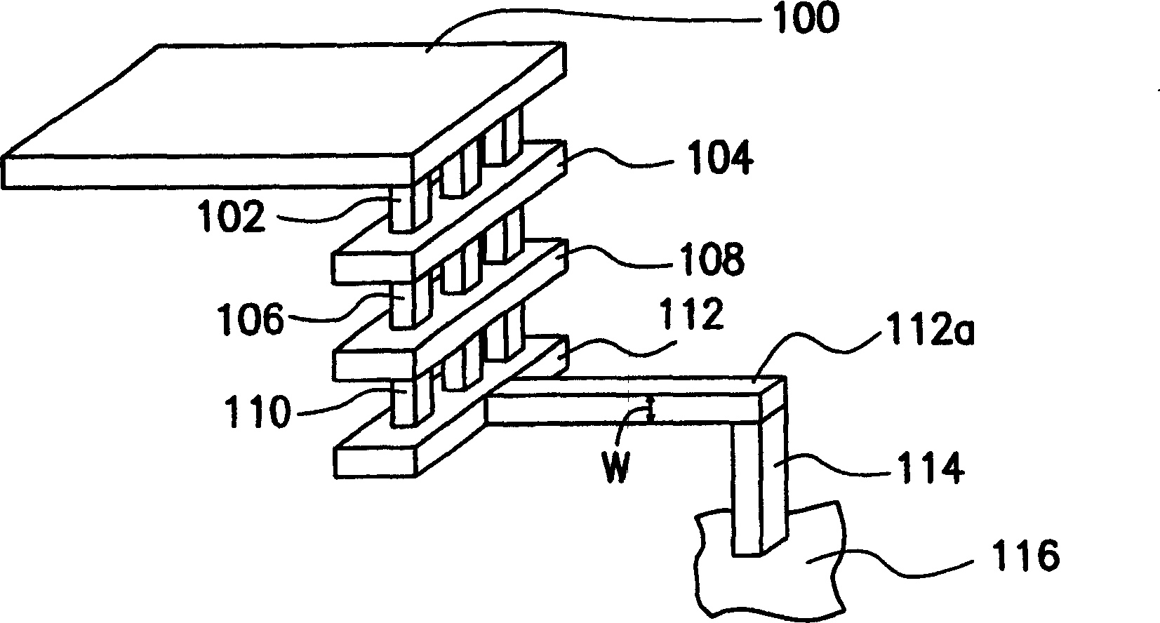
[0027] image 3 It is a cross-sectional view of the circuit connection between the solder pad of the semiconductor element and the electrostatic discharge protection circuit according to the preferred embodiment of the present invention, and Figure 4 It is a perspective view of the circuit connection between the solder pad of the semiconductor element and the electrostatic discharge protection circuit according to the preferred embodiment of the present invention.

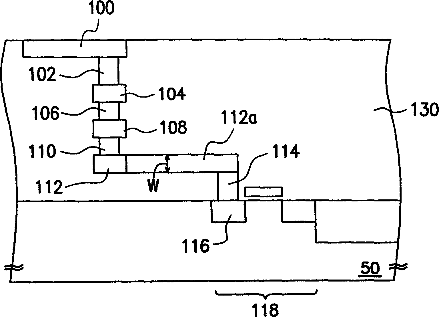
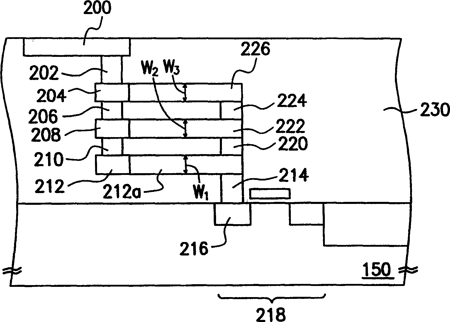
[0028] Please also refer to image 3 and Figure 4 . The external circuit structure of the connection pad 200 and the electrostatic discharge protection circuit 218 of the present invention includes: a via 202, a conductive layer 204, a via 206, a conductive layer 208, a via 210, a conductive layer 212, and as an extension wire The wire 212a, the contact 214, the via 220, the wire 222 as a dummy wire, the via 224, and the wire 226 as a dummy wire.

[0029] exist image 3 and Figure 4 Among them, the bonding...


PUM


Abstract

A circuit structure for connecting a pad and an electrostatic discharge protection circuit. The circuit structure includes: multi-layer conductor layers arranged in parallel between the pad and the base at different heights. The multi-layer first via is electrically connected to the conductor layer of the pad and the adjacent pad, and is electrically connected to each adjacent conductor layer. The first wire is electrically connected to the conductor layer closest to the substrate, and is electrically connected to the drain of the electrostatic discharge protection circuit. A plurality of second wires are arranged in parallel between the first wire and the welding pad at different heights, and each second wire is electrically connected to a conductor layer with a different height. The multi-layer second via window electrically connects the first wire and the second wire adjacent to the first wire, and electrically connects each adjacent second wire.

Description

technical field [0001] The present invention relates to a circuit structure connecting a pad and an electrostatic discharge protection (ESD protection, ESD protection) circuit, and in particular to a circuit that connects a pad and an electrostatic discharge protection circuit to form a multilayer Path (multiple paths) structure, and shunting through multi-layer paths to increase the ESD protection capability of components. Background technique [0002] Electrostatic discharge is the phenomenon of movement of static electricity from non-conductive surfaces that can cause damage to semiconductors and other circuit components in an IC. For example, a human body walking on a carpet can detect a static voltage of several hundred to several thousand volts in the case of high relative humidity (RH), and a static voltage of about several hundred to several thousand volts in the case of low relative humidity. With a static voltage of more than 10,000 volts. A machine for packaging...

Claims


Application Information

Patent Timeline
Patent Type & Authority Patents(China)
IPC IPC(8): H01L23/60H01L23/62H01L23/485
CPCH01L23/60H01L24/05H01L2224/023H01L2224/05093H01L2224/05553H01L2924/01005H01L2924/01006H01L2924/01014H01L2924/01029H01L2924/01033H01L2924/01045H01L2924/01074H01L2924/01082H01L2924/10253H01L2924/14H01L2924/19043H01L2924/00H01L2924/0001
Inventor 黄绍璋周金陶
Owner UNITED MICROELECTRONICS CORP
Features
  • Generate Ideas
  • Intellectual Property
  • Life Sciences
  • Materials
  • Tech Scout
  • Unparalleled Data Quality
  • Higher Quality Content
  • 60% Fewer Hallucinations
Learn More