

SRAM unit with multi-grid transistor and mfg method thereof
A technology for static random access and memory cells, which is applied in semiconductor/solid-state device manufacturing, transistors, electrical components, etc., and can solve problems such as increasing the complexity of circuit design
- Summary
- Abstract
- Description
- Claims
- Application Information
AI Technical Summary
Problems solved by technology
Method used
Image

Examples
no. 1 example
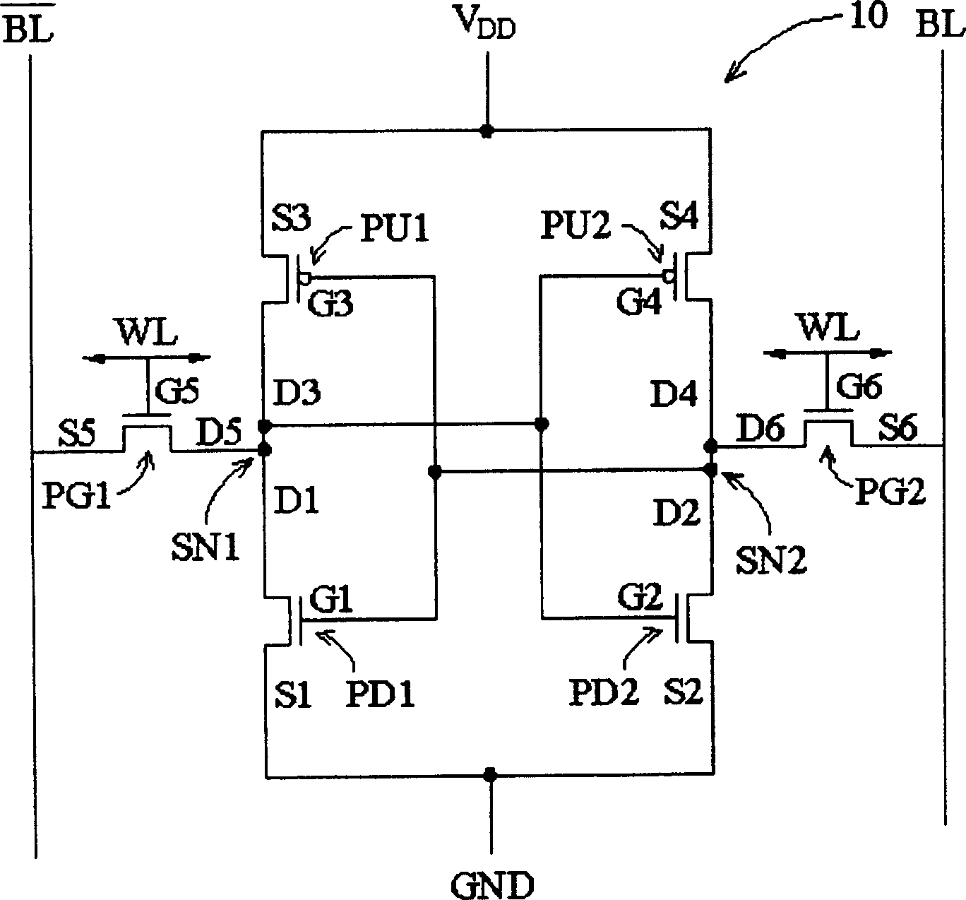
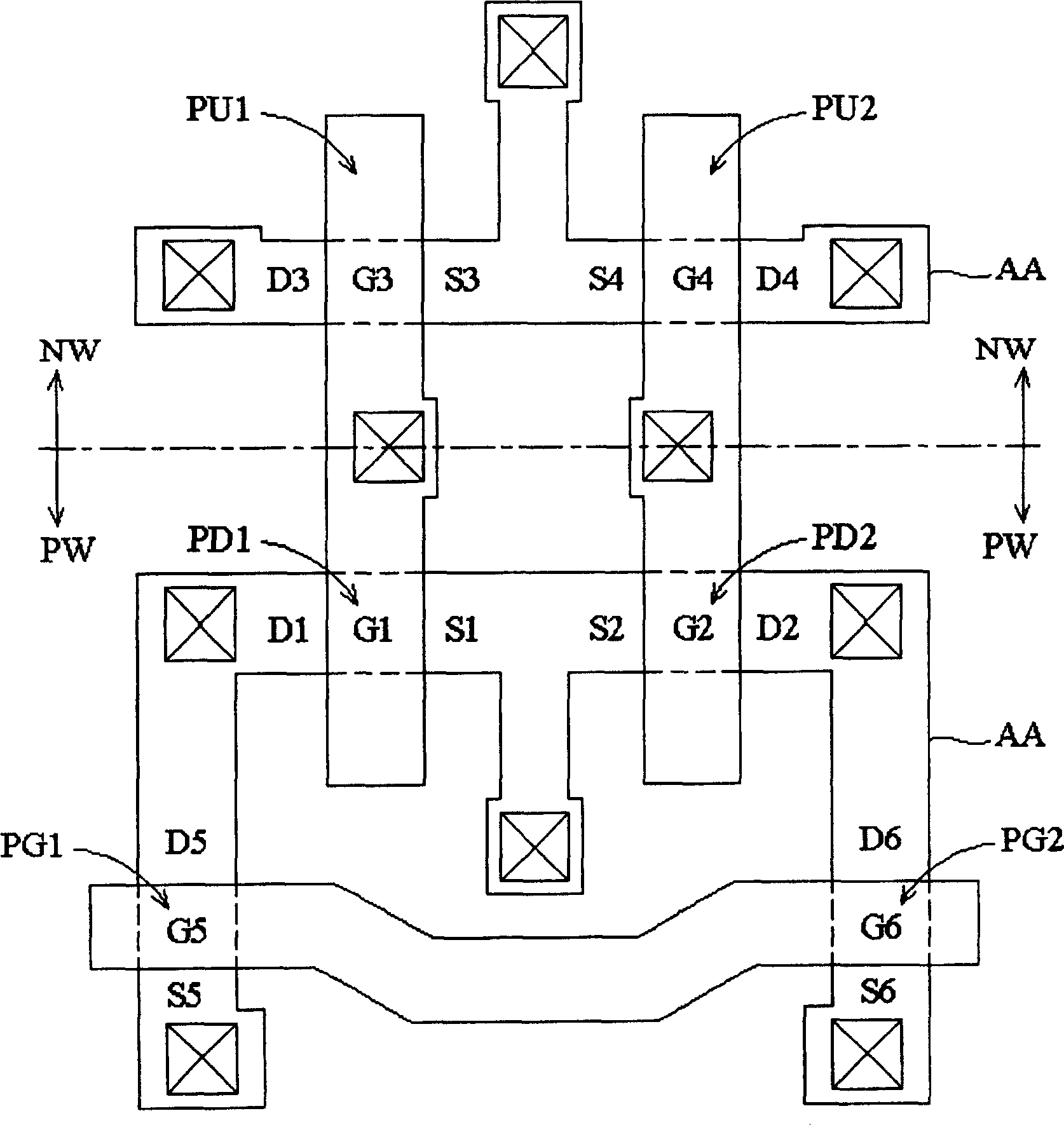
[0103] Structure of SRAM memory cell
[0104] Figure 6C It is a layout diagram of a SRAM memory cell according to a first embodiment of the present invention, which includes the relative configuration relationship of island-shaped semiconductor active regions, source electrodes, drain electrodes, contact window plugs and gate electrodes.
[0105] A 6T-SRAM memory cell basically includes a pair of pull-up transistors PU1 and PU2, a pair of pull-down transistors PD1 and PD2, and a pair of access transistors PG1 and PG2. The pull-up transistors PU1 and PU2 are usually p-channel field effect transistors (PFETs) arranged in the n-type well region NW, and the pull-down transistors PD1 and PD2 and the access transistors PG1 and PG2 are usually n-channel field effect transistors (PFETs) arranged in the p-type well region PW. Channel Field Effect Transistor (NFET).
[0106] The above six transistors are multiple-gate transistors disposed in the island-shaped semiconductor active are...
no. 2 example
[0159] Structure of SRAM memory cell
[0160] Figure 13B It is a layout diagram of an SRAM storage unit according to a second embodiment of the present invention.
[0161] The six transistors in the 6T-SRAM are multi-gate transistors disposed in the island-shaped semiconductor layer 64, such as double-gate transistors (see Figure 7A and Figure 7B ), triple gate transistors (see Figure 8A and Figure 8B ), or Ω-shaped multiple-gate transistors (see Figure 9A and Figure 9B ). Figure 14 It is a perspective view showing the relative arrangement relationship between the island-shaped semiconductor active region and the gate electrode of the access transistor PG1 and the pull-down transistor PD1 composed of double-gate transistors. Figure 15 It is a perspective view showing the relative arrangement relationship between the island-shaped semiconductor active region and the gate electrode of the access transistor PG1 and the pull-down transistor PD1 composed of triple g...
no. 3 example
[0174] Structure of SRAM memory cell
[0175] Figure 16 It is a layout diagram of an SRAM storage unit according to a third embodiment of the present invention. Different from the second embodiment, the island-shaped semiconductor active regions AA of each transistor are separated from each other, and then electrically connected by contact plugs. The numbers in the figure are used Figure 13B The label of , will not be explained here.
[0176] Impedance ratio of pull-down transistor and access transistor (β)
[0177] In the above example, the case where each strip structure in the island-shaped semiconductor active region AA is equal in width and height is taken as an example. Of course, its width and height can be changed depending on the actual layout considerations. But usually the height will be equal due to the convenience of the manufacturing process. In addition, generally, the bottom contribution width of the island-shaped semiconductor layer 64 is also equal in...
PUM
 Abstract
Description
Claims
Application Information