Supercharge Your Innovation With Domain-Expert AI Agents!

Method for growing high-mobility gallium nitride epitaxial film

A high-mobility, gallium nitride technology, applied in the field of epitaxial growth of gallium nitride epitaxial film, can solve the problems of GaN material crystal quality degradation, destruction of GaN lattice, and affecting device performance

Inactive Publication Date: 2007-05-02
INST OF SEMICONDUCTORS - CHINESE ACAD OF SCI
View PDF1 Cites 0 Cited by
  • Summary
  • Abstract
  • Description
  • Claims
  • Application Information

AI Technical Summary

Problems solved by technology

If the doping method is used, although the doped atoms can improve the mobility of the GaN material, the doped atoms destroy the original crystal lattice of GaN, resulting in a decrease in the crystal quality of the GaN material
Therefore, this method will affect the performance of the material itself and the device fabricated from it.

Method used


Image

  • Method for growing high-mobility gallium nitride epitaxial film
  • Method for growing high-mobility gallium nitride epitaxial film
  • Method for growing high-mobility gallium nitride epitaxial film

Examples


Embodiment

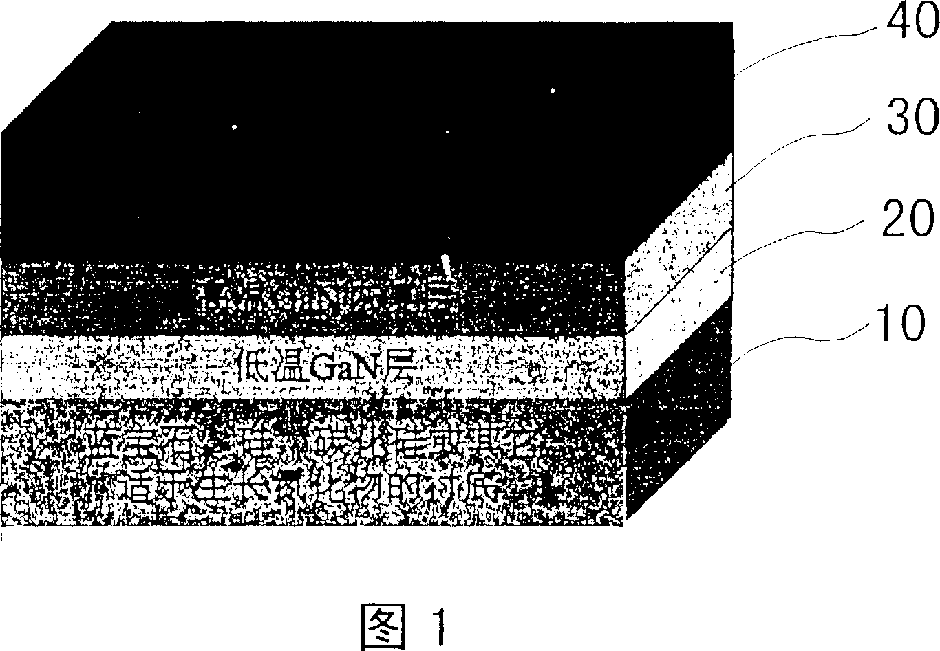
[0025] Referring to Fig. 1, a method for growing a high-mobility gallium nitride epitaxial film of the present invention comprises the following steps:

[0026] 1. On the substrate 10 sapphire (0001) or silicon (111) or silicon carbide (0001) or other substrates suitable for growing nitrides such as GaLiO 3 A low-temperature GaN nucleation layer is grown on the crystal surface of , ZnO, etc. by metal-organic chemical vapor deposition (MOCVD). The substrate temperature is about 500-600° C., the pressure is 400-600 torr, and the growth thickness is 0.01-0.06 μm.

[0027] 2. Afterwards, the temperature of the substrate 10 is increased to grow the gallium nitride recovery layer. The growth temperature of the gallium nitride recovery layer is between 1000-1100° C., the growth pressure is 100-300 torr, and the growth thickness is 0.1-0.3 μm.

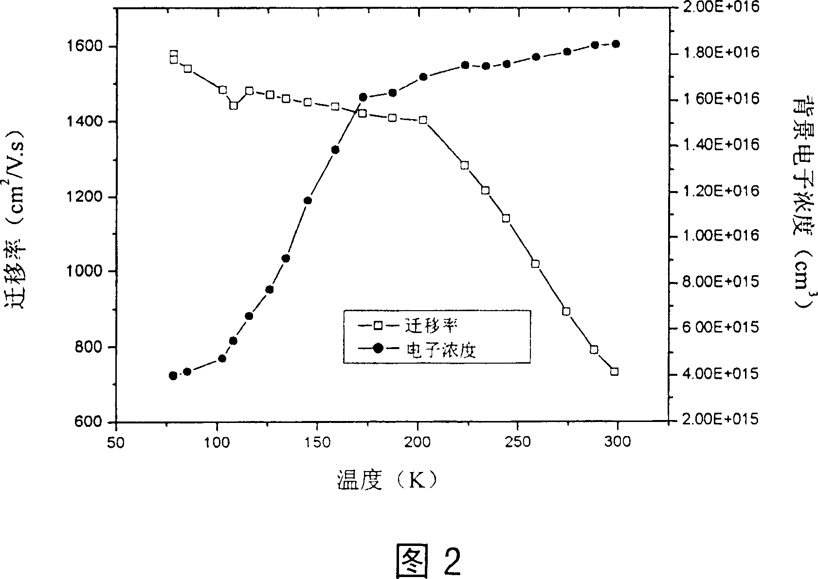
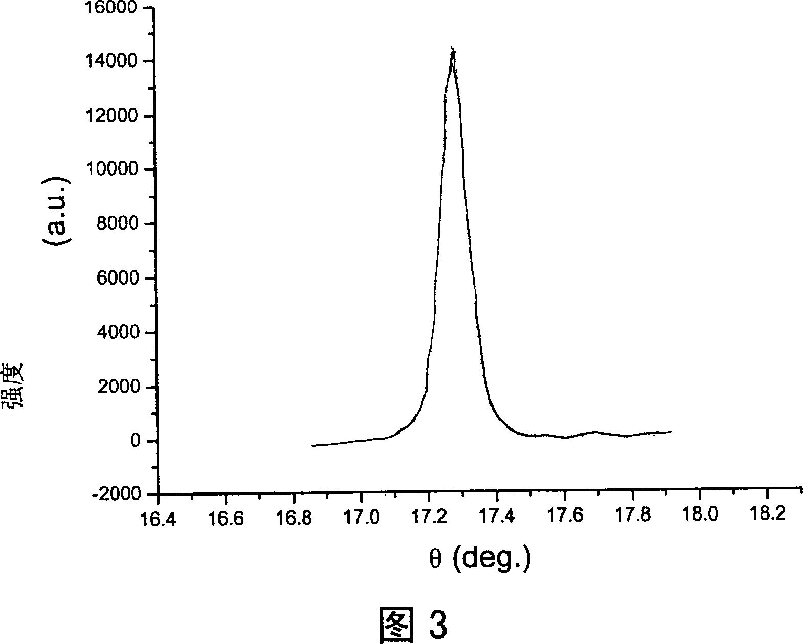
[0028] 3. Finally, change the growth chamber pressure, unintentionally dope the high-mobility gallium nitride layer, the growth temperature ...


PUM

PropertyMeasurementUnit
temperatureaaaaaaaaaa
pressureaaaaaaaaaa
thicknessaaaaaaaaaa

Abstract

The invention provides a method for growing high-mobility gallium nitride epitaxial film, characterized in that the method comprises the following steps, selecting a substrate, growing a layer of low-temperature gallium nitride core formation onto the substrate with a metallorganic chemical vapor deposition method, elevating the temperature of the substrate, growing a gallium nitride recovery layer onto the low-temperature gallium nitride core formation layer, finally changing growth chamber pressure, growing a high mobility gallium nitride layer on the gallium nitride recovery layer.

Description

technical field [0001] The invention belongs to the technical field of semiconductors, in particular to the mobility at room temperature not less than 400cm 2 / V.s GaN epitaxial film epitaxial growth method. Background technique [0002] As a typical representative of the third-generation semiconductor materials, III-V gallium nitride materials have great application prospects in the fields of optoelectronics and microelectronics due to their unique physical, chemical and mechanical properties. GaN materials can be used to prepare HEMT, HFET, HBT, JFET, MOSFET, SAW and other devices. Mobility is an important parameter to characterize the quality of materials, and the acquisition of high mobility materials is of great benefit to material research and device development. However, due to the lack of heterogeneous substrate materials that match GaN materials, the purity of the materials is difficult to improve, so it is difficult to obtain GaN materials with high mobility. ...

Claims


Application Information

Patent Timeline
Patent Type & Authority Patents(China)
IPC IPC(8): C30B25/02C30B29/40H01L21/205
Inventor 王晓亮胡国新王军喜李建平曾一平李晋闽
Owner INST OF SEMICONDUCTORS - CHINESE ACAD OF SCI
Features
  • R&D
  • Intellectual Property
  • Life Sciences
  • Materials
  • Tech Scout
  • Unparalleled Data Quality
  • Higher Quality Content
  • 60% Fewer Hallucinations
Learn More