
Contact structure member and production method thereof, and probe contact assembly using said contact structure member

A technology for contacting components and contacting components, which is applied to contact components, measuring leads/probes, components of connecting devices, etc., can solve problems such as inconsistent quality, and achieve the effects of low cost, high reliability and high efficiency

Inactive Publication Date: 2002-05-22
株式会社鼎新
View PDF0 Cites 18 Cited by
  • Summary
  • Abstract
  • Description
  • Claims
  • Application Information

AI Technical Summary

Problems solved by technology

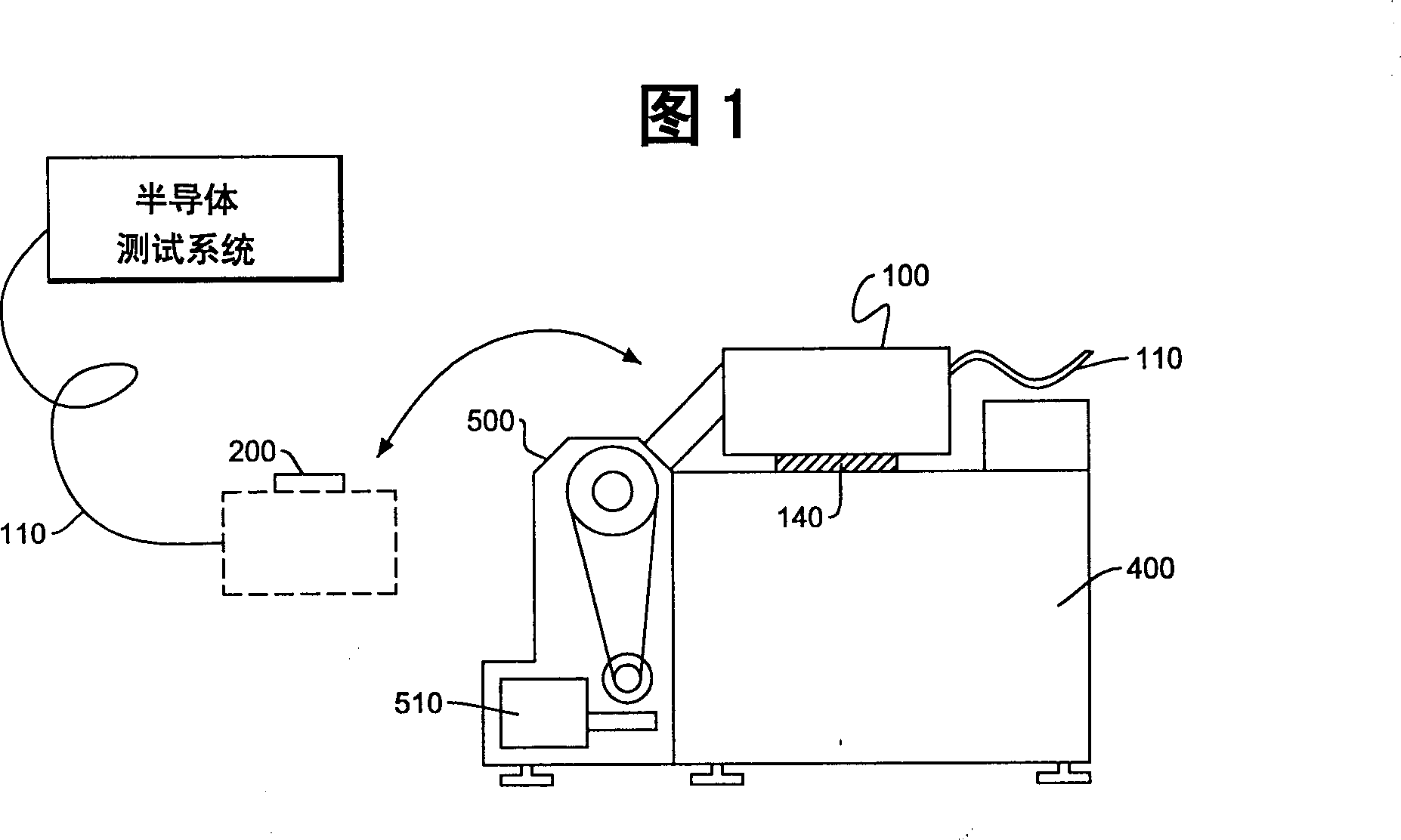
[0015] In conventional technology, probe cards such as image 3 As shown, are handmade resulting in inconsistent quality

Method used


Image

  • Contact structure member and production method thereof, and probe contact assembly using said contact structure member
  • Contact structure member and production method thereof, and probe contact assembly using said contact structure member
  • Contact structure member and production method thereof, and probe contact assembly using said contact structure member

Examples


Embodiment Construction

[0078] Detailed description of the preferred embodiment

[0079] Figure 5 -7 represents an example of the contact member of the present invention. Please note that the description of the present invention will be annotated with terms including "horizontal", "vertical" and the like. The inventors use these terms to describe the relative positional relationship of elements related to the invention. Therefore, terms like "horizontal" and "vertical" should not be read only narrowly as "ground-level" or "gravity-vertical".

[0080] The contact member is constituted by a contact substrate 20 and contacts 30 . exist Figure 5 example, each contactor 30 1 Extending substantially in the vertical direction, and forming: a middle portion, the middle portion is connected to the contact substrate 20; a contact portion, at Figure 5 wherein the lower end thereof is preferably pointed; a first spring portion, located between the middle portion and the contact portio...


PUM


Abstract

A method of producing a contact structure for establishing electrical connection with contact targets. The contact structure is formed of a contact substrate and a plurality of contactors. The contactor has a contact portion which is oriented in a vertical direction to form a contact point, an intermediate portion which is inserted in a through hole provided on the contact substrate, and a base portion having a base end which functions as a contact pad and a spring portion provided between the base end and the intermediate portion for producing a resilient contact force when the contactor is pressed against the contact target.

Description

field of invention [0001] The invention relates to a contact member, a production method thereof, and a probe contact assembly using the contact member. More specifically, the present invention relates to a contact member having a large number of contacts in a vertical direction. The present invention further relates to a method for producing a large number of contacts on a semiconductor wafer in the horizontal direction, and removing the contacts mounted on the substrate from the wafer in the vertical direction to form a contact structure, for example, Contact probe assemblies, probe cards, IC chips, or other contact mechanisms. background of the invention [0002] When testing high-density and high-speed electronic devices such as LSI (Large Scale Integration) and VLSI (Very Large Scale Integration), high-performance contact members such as probe cards having a large number of contacts must be used. In other applications, the contact members can be used ...

Claims


Application Information

Patent Timeline
Patent Type & Authority Applications(China)
IPC IPC(8): G01R31/26G01R1/067G01R1/073G01R3/00G01R31/28H01L21/302H01L21/48H01L21/66H01L23/485H01R12/00H01R13/24H05K3/20H05K3/40
CPCG01R1/06733H01L2924/01032H05K3/4015G01R1/06711G01R1/07307H01L2924/01046H01L2924/01082H01R13/2407H01L2924/01004H01R2201/20H01L2924/01045G01R3/00H01L2924/09701H01L2924/30105H01L2924/01019G01R1/07378H01L2924/01029H01L2224/13099H01L2924/01022H01L2924/01027H01L2924/19041H01L2924/01013H01L2924/30107H01L2924/01039H01L2924/01056H01L2924/01024H01R13/2428G01R1/06716G01R1/06772H01L2924/3011H01L2924/01068H01L2924/14H01L2924/19042H01L2924/01005H01L2924/01033H01L2924/01006H01L21/4885H01R12/57H01L2924/01074H01L2924/01078H01L2924/10253G01R1/07314H01L24/10H05K3/20G01R1/06727H01L24/13H01L2924/15787H01L2924/12042H01L2224/13H01L2224/05573H01L2224/05568H01L2924/00014H01L2924/00H01L2224/05599G01R1/067
Inventor 周豫余大江罗伯特·爱德华·阿尔达斯西奥多·A·库利
Owner 株式会社鼎新
Learn More