Over-all wiring method for standard units based on optimized time delay and key network techniques

A technology of overall wiring and network technology, which is applied in the field of overall wiring of standard cells, and can solve problems such as inability to reflect circuit overtime, strict constraints on intermediate wiring results, and inability to realize active control, etc.

Inactive Publication Date: 2002-07-24
TSINGHUA UNIV
View PDF0 Cites 14 Cited by
  • Summary
  • Abstract
  • Description
  • Claims
  • Application Information

AI Technical Summary

Problems solved by technology

Method (1) has a certain blindness in the allocation of delay constraints, and often the delay allocation results do not match the actual wiring requirements, making it impossible to improve the crowded line network
Method (2) uses the greedy trial method to determine the blindness of the line network that needs to improve the delay, and cannot realize active control
At the same time, the total number of critical paths is generally large, and all critica...

Method used


Image

  • Over-all wiring method for standard units based on optimized time delay and key network techniques
  • Over-all wiring method for standard units based on optimized time delay and key network techniques
  • Over-all wiring method for standard units based on optimized time delay and key network techniques

Examples


Embodiment Construction

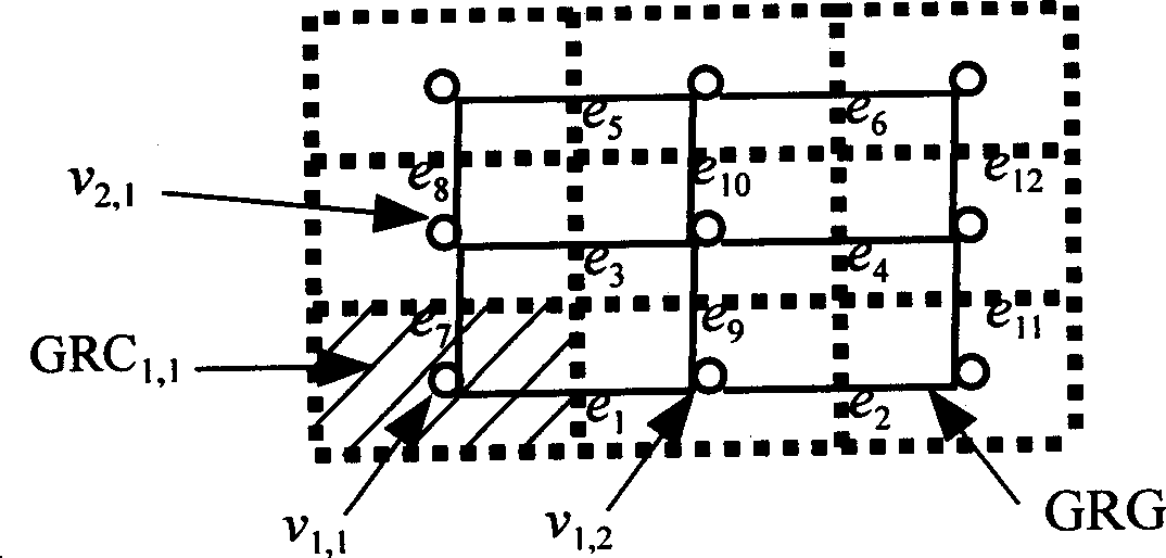
[0062] For the current multi-layer wiring technology in VLSI design, the routing area is no longer a wiring channel between units, but a complete chip plane. The grid method can be used to divide the entire chip plane into several regions called the overall wiring unit GRC according to rows and columns, and then generate the dual graph of the GRC, that is, as figure 1 Shown in the general wiring diagram GRG. GRG by N nr ×N nc nodes and the edges connecting these nodes. with GRC nr,nc The corresponding node v nr,nc The coordinates are GRC nr,nc the center point of . connect two nodes v nr1,nc1 and v nr2,nc2 The edge of is called e k ; l k represents two nodes v nr1,nc1 and v nr2,nc2 The distance between, called e k length; C k represents two nodes v nr1,nc1 and v nr2,nc2 The number of connections of the line network that can pass through the adjacent sides of the corresponding two GRCs is called e k capacity. Therefore, the pin point Pin to be connected in the...


PUM


Abstract

An over-all wiring method for standard units with optimized time delay includes creating over-all wiring diagram, configuring initial wiring tree with the shortest length, configuring key network composed of key pins, key sides and the weight, virtual source point and convergent point of each orientative side, reconfiguring the wiring tree from a group of sides with minimal division for reducing time delay, comparing the given delay data with optimized delay, and iterating to obtain wiring tree of over-all network.

Description

technical field [0001] A standard cell general wiring method based on key network technology to optimize time delay belongs to the field of computer aided design of integrated circuits, in particular to the field of standard cell general wiring. Background technique [0002] In the VLSI design of VLSI, the physical design is the main link in the VLSI design process. The related computer-aided design technology is called layout design, and the overall wiring has a great influence on the success of the final detailed wiring and the performance of the chip. At present, the manufacturing process of integrated circuits has entered the stage from deep submicron DSM to ultra-deep submicron VDSM, and the design scale of integrated circuits is also developing from ultra-large-scale VLSI, very large-scale ULSI to G-large-scale GSI. At this time, interconnection Line delay has surpassed gate delay to become the main factor affecting chip performance. Therefore, not only to optimize t...

Claims


Application Information

Patent Timeline
IPC IPC(8): G06F17/50
Inventor 洪先龙经彤鲍海云蔡懿慈许静宇
Owner TSINGHUA UNIV
Why Eureka
Try Eureka