Communication device
A communication device and bias technology, applied in automatic frequency control, electrical components, pulse technology, etc., can solve problems such as cut-off hysteresis
- Summary
- Abstract
- Description
- Claims
- Application Information
AI Technical Summary
Problems solved by technology
Method used
Image

Examples
Embodiment 1
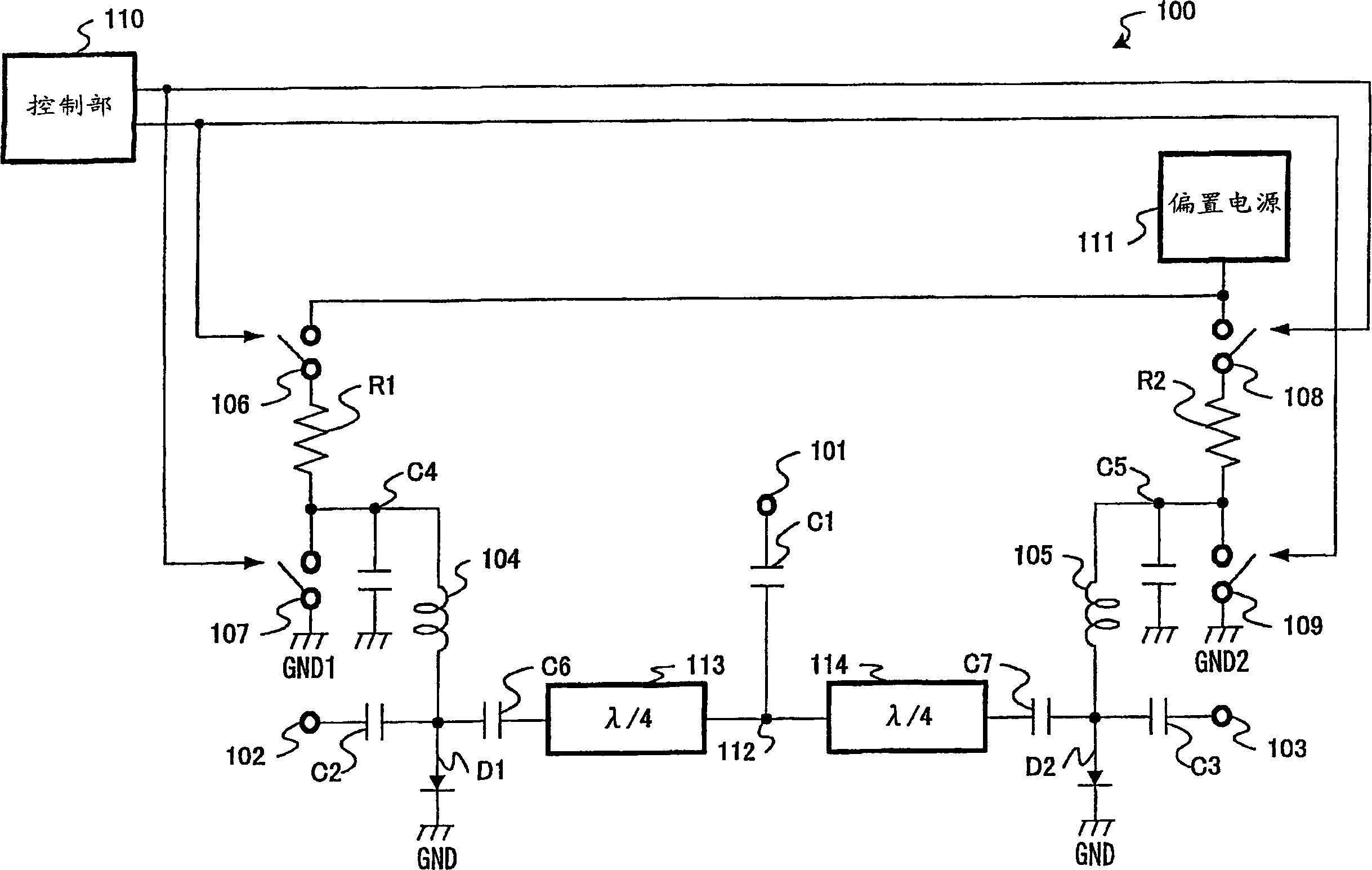
[0025] figure 1 It is a circuit diagram of the high-frequency switch of Embodiment 1 of the present invention. Here, PIN diodes D1 and D2 are used as the first and second switching elements.
[0026] The high-frequency switch 100 is formed by the branch point 112 of the path from the first terminal 101 through the DC blocking capacitor C1, through the λ / 4 wavelength lines 113, 114 with the length of 1 / 4 wavelength of the center frequency, and the DC blocking capacitors C6, C7 , PIN diodes D1 and D2 with the other end grounded are installed in parallel, and then connected to the second terminal 102 and the third terminal 103 via DC blocking capacitors C2 and C3.
[0027] The λ / 4 wavelength lines 113 and 114 have a line length of 1 / 4 of the wavelength λ of the main high-frequency signal passing through the transmission line, thereby matching input and output impedances and preventing reflected waves from being generated.
[0028] A bias current is supplied from a bias power su...
Embodiment 2
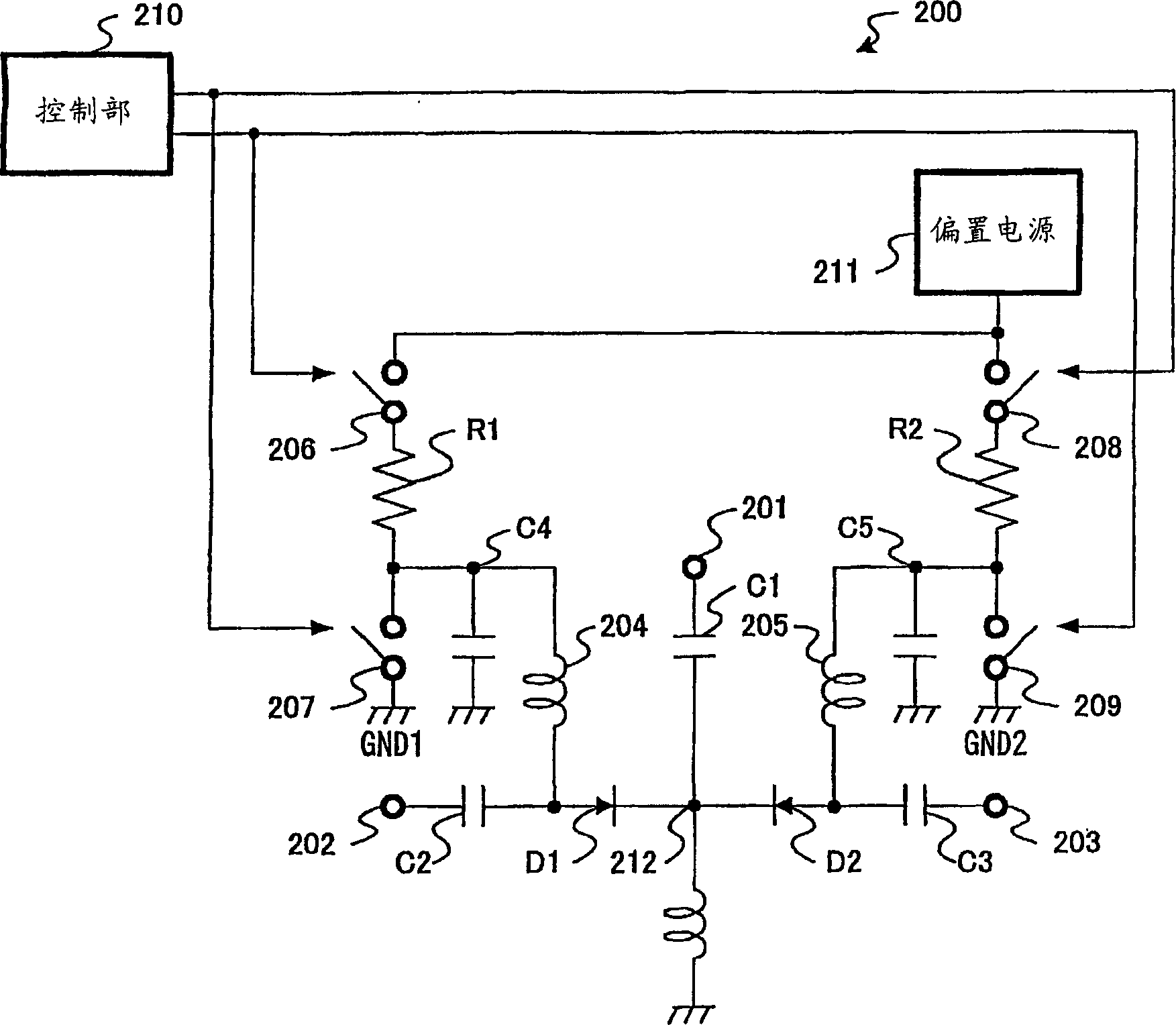
[0036] figure 2 It is a circuit diagram of the high-frequency switch of Embodiment 2 of the present invention. Here, PIN diodes D1 and D2 are also used as the first and second switching elements.
[0037] The high frequency switch 200 is connected to the second terminal 202 and the third terminal 203 through the DC blocking capacitors C2 and C3 by connecting the PIN diodes D1 and D2 in series at the branch point 212 of the path from the first terminal 201 through the DC blocking capacitor C1.
[0038] The bias current is supplied from the bias power supply 211 to the PIN diodes D1 and D2 via the bias lines 204 and 205 , the resistors R1 and R2 , and the switches 206 and 208 . The bias lines 204 and 205 have a length of 1 / 4 wavelength of the center frequency, and are short-circuited at high frequency by capacitors C4 and C5 that have low impedance to the center frequency.
[0039] Furthermore, switches 207, 209 are provided between the bias lines 204, 205 and grounds GND1, G...
Embodiment 3
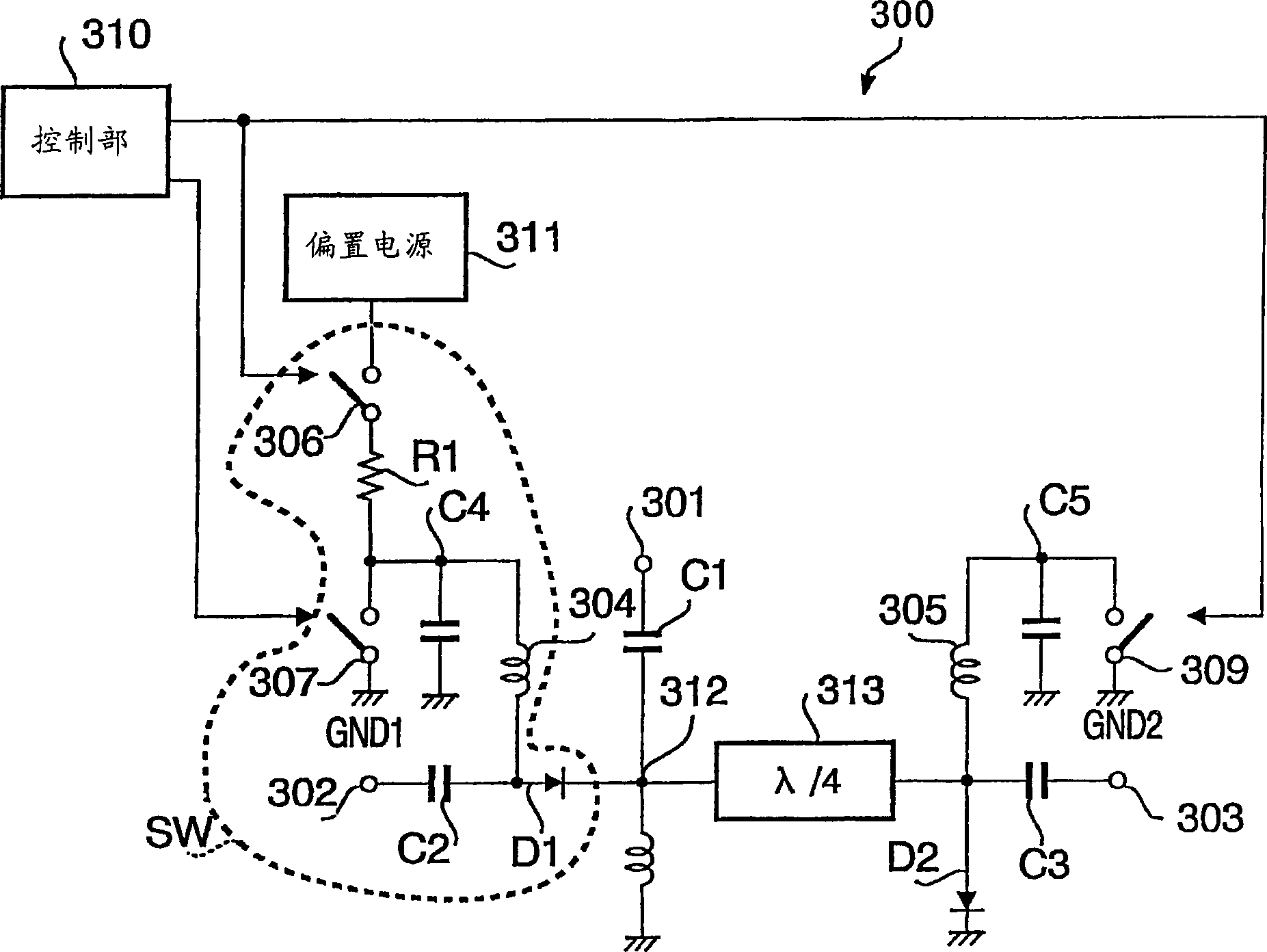
[0044] image 3It is a circuit diagram of the high-frequency switch of Embodiment 3 of the present invention. Here, PIN diodes D1 and D2 are also used as the first and second switching elements.
[0045] The high-frequency switch 300 is connected to the second terminal 302 through the DC blocking capacitor C2 through the branch point 312 of the path from the first terminal 301 through the DC blocking capacitor C1, and has a center frequency of 1 / 4. A λ / 4 wavelength line 313 with a wavelength length of λ / 4 is installed in parallel with a PIN diode D2 that connects the other end to ground, and is connected to the third terminal 303 through a DC blocking capacitor C3.
[0046] A bias power supply 311 is connected to the PIN diode D1 via a bias circuit 304 , a resistor R1 and a switch 306 . In addition, a bias line 305 is connected to the PIN diode D2.
[0047] The bias lines 304 and 305 have a length of 1 / 4 wavelength of the center frequency, and are short-circuited at high fr...
PUM
 Abstract
Description
Claims
Application Information
 - R&D
- Intellectual Property
- Life Sciences
- Materials
- Tech Scout
- Unparalleled Data Quality
- Higher Quality Content
- 60% Fewer Hallucinations
Browse by: Latest US Patents, China's latest patents, Technical Efficacy Thesaurus, Application Domain, Technology Topic, Popular Technical Reports.
© 2025 PatSnap. All rights reserved.Legal|Privacy policy|Modern Slavery Act Transparency Statement|Sitemap|About US| Contact US: help@patsnap.com