Supercharge Your Innovation With Domain-Expert AI Agents!

Mixed integrated circuit device and its manufacturing method

一种混合集成电路、制造方法的技术,应用在印刷电路制造、电路、印刷电路等方向,能够解决接合时间长、易折曲、Al细线弹性差等问题,达到提高散热性、解决现有问题的效果

Inactive Publication Date: 2003-02-05
SANYO ELECTRIC CO LTD
View PDF1 Cites 12 Cited by
  • Summary
  • Abstract
  • Description
  • Claims
  • Application Information

AI Technical Summary

Problems solved by technology

This is because Al thin wires have poor elasticity and are easy to bend. Ultrasonic waves are required for bonding, so the bonding time is long, so it cannot be used.

Method used


Image

  • Mixed integrated circuit device and its manufacturing method
  • Mixed integrated circuit device and its manufacturing method
  • Mixed integrated circuit device and its manufacturing method

Examples


Embodiment Construction

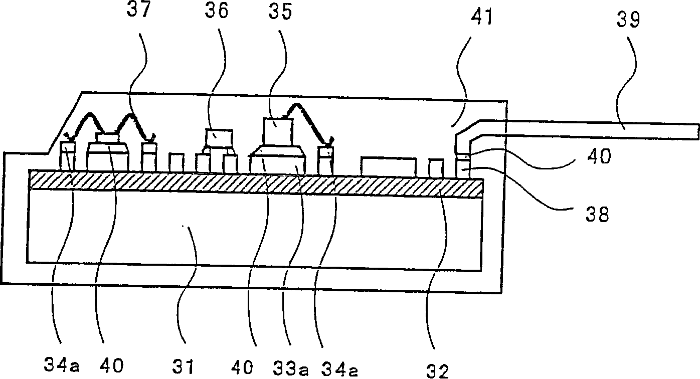
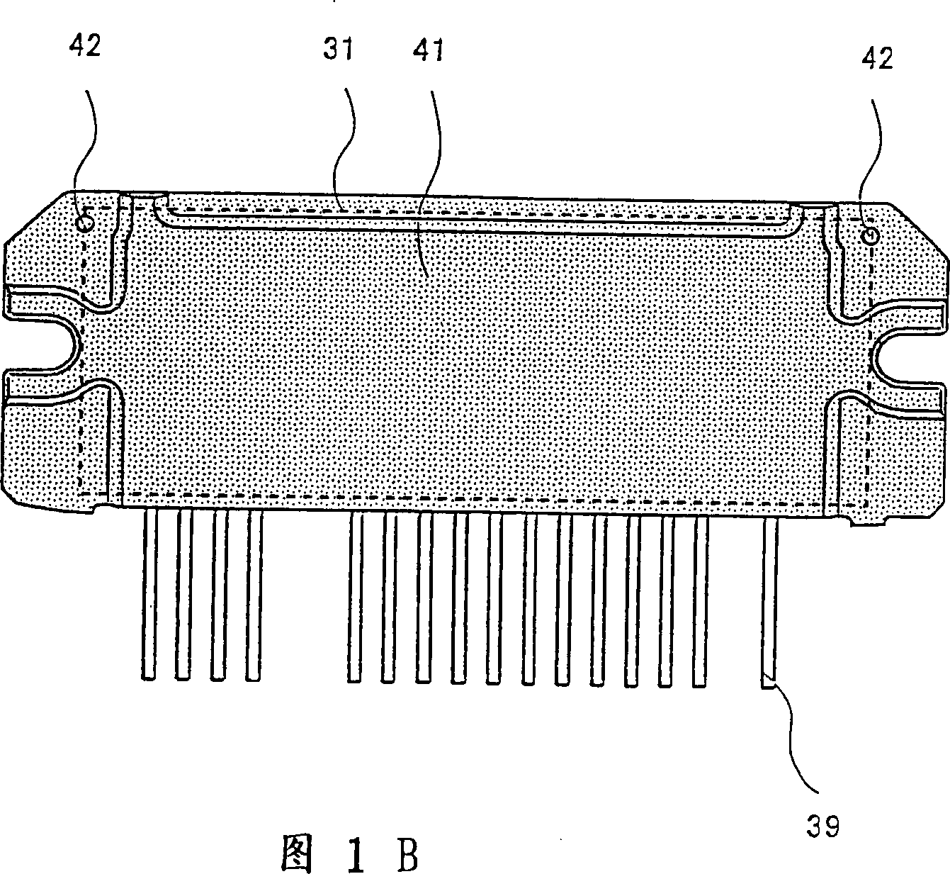
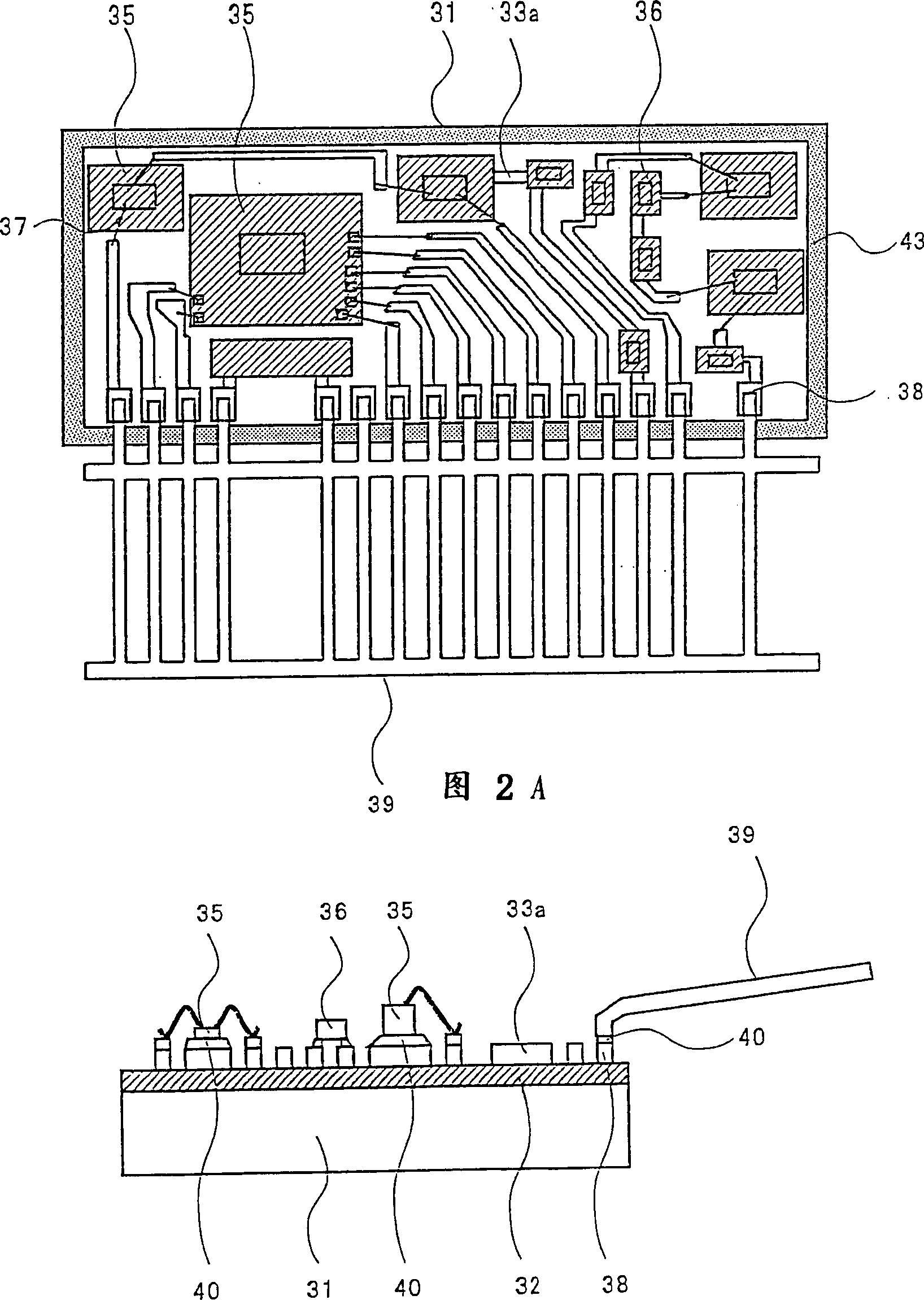
[0055] Below, refer to Figure 1A , Figure 1B and Figure 2A, Figure 2B A hybrid integrated circuit device according to Embodiment 1 of the present invention will be described.

[0056] First, refer to Figure 1A , FIG. 1B illustrates the structure of the hybrid integrated circuit device. Such as Figure 1A As shown, the hybrid integrated circuit device 31 adopts a substrate with good heat dissipation in consideration of heat generated by semiconductor elements etc. fixedly mounted on the substrate 31 . In this embodiment, the case where the aluminum substrate 31 is used will be described. In addition, although an aluminum (hereinafter referred to as Al) substrate is used for the substrate 31 in this embodiment, it does not need to be particularly limited. For example, this embodiment can also be realized by using a printed circuit board, a ceramic substrate, a metal substrate, etc. as the substrate 31 . Moreover, a copper substrate, an iron substrate, an iron-nickel sub...


PUM


Abstract

In a molding process, a hybrid integrated circuit substrate is fixed the position of the substrate in a thickness direction. A leadframe is connected, with an upward inclination, to a hybrid integrated circuit substrate and transported into a mold cavity. By horizontally fixing the leadframe by mold dies, the hybrid integrated circuit substrate inclined upward is urged downward by a pushpin. This can fix the position of the hybrid integrated circuit substrate within the mold cavity and integrally transfer-molded.

Description

technical field [0001] The present invention relates to a hybrid integrated circuit device and its manufacturing method, and relates to a hybrid integrated circuit device in which a resin package is formed by transfer molding on a hybrid integrated circuit substrate and its manufacturing method. Background technique [0002] Generally, there are mainly two packaging methods for hybrid integrated circuit devices. [0003] The first method is to package with a device in the shape of a lid placed on a hybrid integrated circuit substrate on which circuit elements such as semiconductor devices are mounted, that is, a device generally called a box member. The structure sometimes adopts a hollow structure or a structure in which resin is additionally injected. [0004] The second method is injection molding, which is a molding method of semiconductor ICs. For example, it is shown in JP-A-11-330317. The injection molding method generally uses a thermoplastic resin, for example, a...

Claims


Application Information

Patent Timeline
Patent Type & Authority Applications(China)
IPC IPC(8): H01L23/28H01L21/56H01L23/31H01L23/433H05K3/28
CPCH01L23/4334H01L2224/45124H01L23/3135H01L2924/01078H01L2924/19041H01L2224/45144H01L2924/01079H05K3/284H01L24/48H01L2924/3025H01L2224/48227H01L21/565H01L2224/45015H01L24/45H01L2924/14H01L2924/181H01L2224/05554H01L2224/73265H01L2924/00014H01L2924/00015H01L2924/00H01L2924/00012
Inventor 饭村纯一大川克实小池保广西塔秀史
Owner SANYO ELECTRIC CO LTD
Features
  • R&D
  • Intellectual Property
  • Life Sciences
  • Materials
  • Tech Scout
  • Unparalleled Data Quality
  • Higher Quality Content
  • 60% Fewer Hallucinations
Learn More