Bipolar insulated-gate transistor device, its preparing process and method for controlling its switching speed

A bipolar transistor and transistor technology, applied in the field of insulated bipolar gate transistor device and its manufacture, controlling its switching rate, power semiconductor device and its manufacture, can solve the problem of increasing forward voltage drop and leakage current of transistor device, Impact and other issues

Inactive Publication Date: 2003-02-12
CHINO EXCEL TECH CORP
View PDF0 Cites 10 Cited by
  • Summary
  • Abstract
  • Description
  • Claims
  • Application Information

AI Technical Summary

Problems solved by technology

However, although the presence of platinum or gold can reduce the lifetime of the minority carriers and improve the switching rate, platinum or gold will dissolve into the silicon crystal, and too much platinum or gold will affect and increase the forward voltage drop of the transistor device and leakage current

Method used


Image

  • Bipolar insulated-gate transistor device, its preparing process and method for controlling its switching speed
  • Bipolar insulated-gate transistor device, its preparing process and method for controlling its switching speed
  • Bipolar insulated-gate transistor device, its preparing process and method for controlling its switching speed

Examples


Embodiment Construction

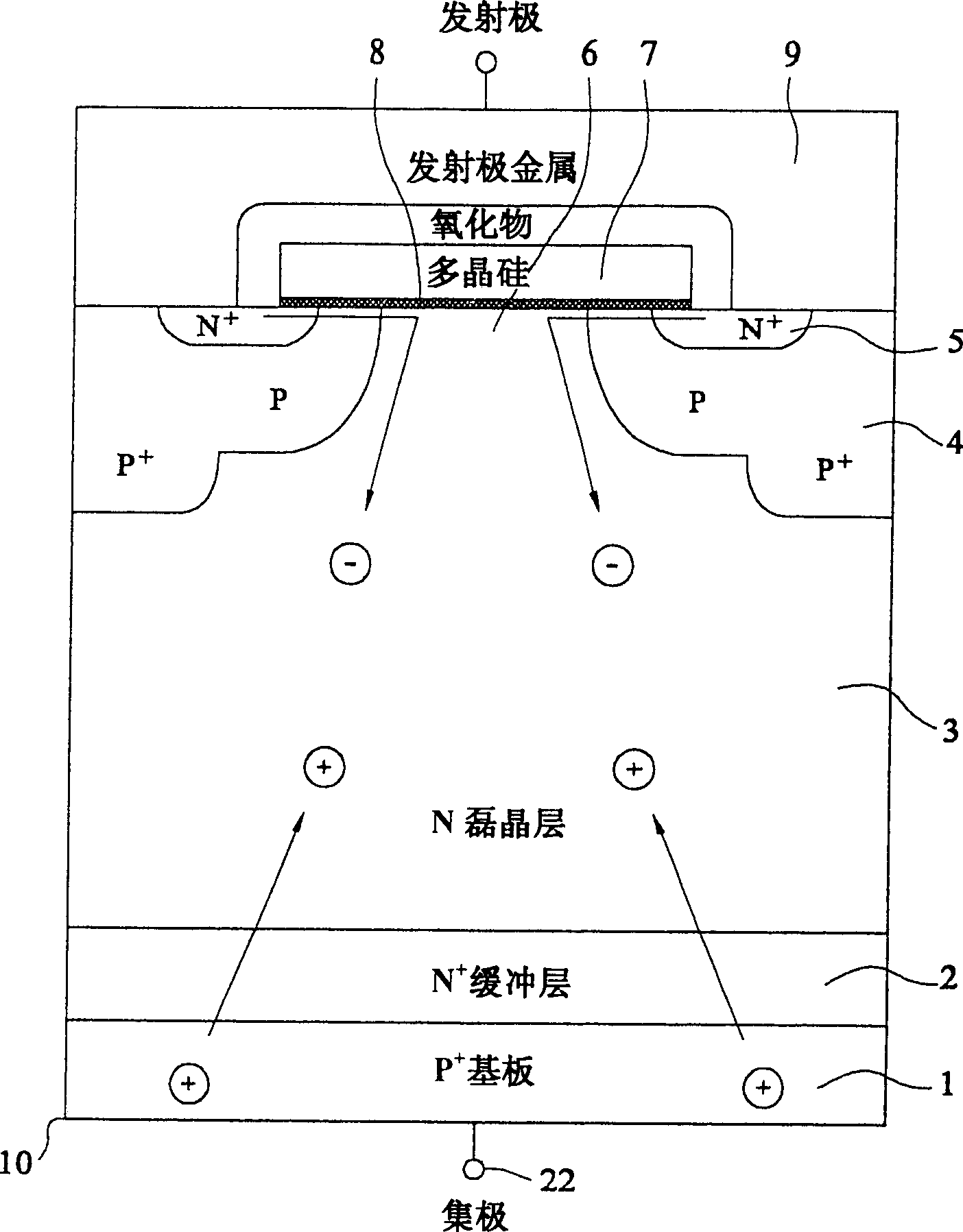
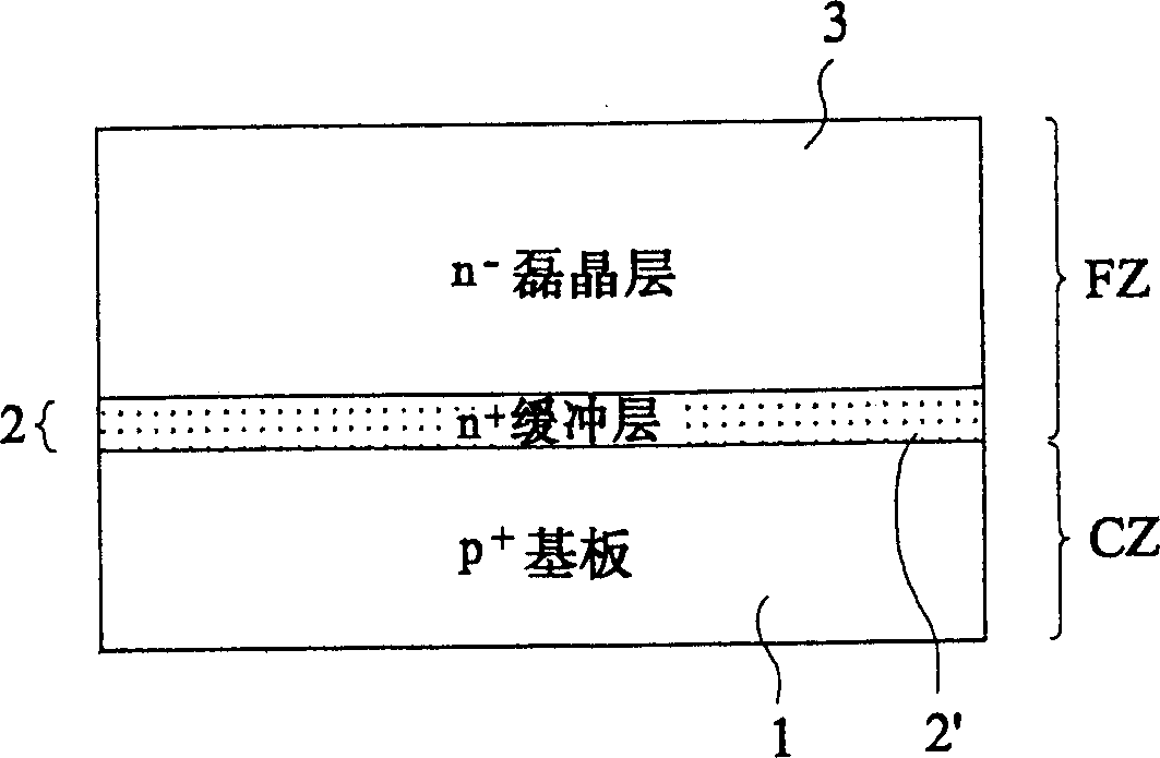
[0026] Such as figure 1 As shown, the present invention provides an IGBT device, wherein a phosphorus-doped n+ buffer layer 2 with a thickness of about 5-12 microns is formed on a p+ silicon substrate 1, and an n+ buffer layer 2 with a thickness of about 60-150 microns -layer 3 is on the n+ buffer layer 2, and the p-type base layer 4 is selectively formed on the upper main surface of the n- epitaxial layer 3, thereby forming a p+ semiconductor layer 1, n-type layer 3 and 2 (n- and n+), and a pnp bipolar transistor of the p-type base layer 4. Further, the n+ emitter region 5 is selectively formed on the upper main surface of the p-type base layer 4; the p-type base region 4 sandwiched by the n-type semiconductor layer 3 and the n+ emitter region 5 The channel region 6 of the upper main surface part is deposited with a gate electrode 7, the gate electrode 7 is a polysilicon structure, and a gate insulating film 8 is contained between the gate electrode 7 and the channel region ...


PUM


Abstract

A bipolar insulated-gate transistor device with high switch speed has sequentially a collector with P+Si base plate n+buffer layer, n-crystal layer, p-type base area selectively formed on the n-crystal layer to obtain bipolar PNP transistor, n+emitter area, and polysilicon grid on the grid oxide layer between n+semiconductor layer and n+emitter area. It also has a dislocation layer generated by doping Ge into n+buffer to shorten the life of minority carriers and in crease the switching speed.

Description

technical field [0001] The present invention relates to a method for controlling the switching rate of an insulated bipolar gate transistor (InsulatedGate Bipolar Transistor, IGBT) device, and an insulated bipolar gate transistor device and its manufacturing method, especially a low conduction Resistive power semiconductor devices, methods of manufacturing the same, and methods for controlling the switching rate thereof. Background technique [0002] figure 1 Shown is a cross-sectional view of a common single-cell n-channel (n-channel) IGBT cell, which is produced by serially connecting a plurality of IBT cells into an IBT device, wherein the The IGBT device can be applied to high voltage and high current switching devices. The n+ buffer layer 2 in each IGBT unit is formed on the p+ silicon substrate 1, and the n- layer 3 is epitaxially grown on the n+ buffer layer 2, while the p-type base layer 4 selectively Formed in the upper main surface of the n- epitaxial layer 3, t...

Claims


Application Information

Patent Timeline
Patent Type & Authority Applications(China)
IPC IPC(8): H01L21/328H01L29/72
Inventor 邱恒德
Owner CHINO EXCEL TECH CORP
Why Eureka
Try Eureka