UMOS transistor capable of modulating on resistance

A technology of on-resistance and transistors, applied in the direction of semiconductor devices, circuits, electrical components, etc., to meet application requirements, reduce drain-source on-resistance, and improve mobility

Inactive Publication Date: 2011-01-26
如皋市生产力促进中心
View PDF0 Cites 0 Cited by
  • Summary
  • Abstract
  • Description
  • Claims
  • Application Information

AI Technical Summary

Problems solved by technology

Although the subsequent proposal of the gradient oxide-bypassed (GOB) structure made the field strength distribution in the drift region of the device flatter, it is still inferior to the OB device in the device design below 60V.

Method used


Image

  • UMOS transistor capable of modulating on resistance
  • UMOS transistor capable of modulating on resistance
  • UMOS transistor capable of modulating on resistance

Examples


Embodiment Construction

[0014] The present invention is described in more detail below in conjunction with accompanying drawing example:

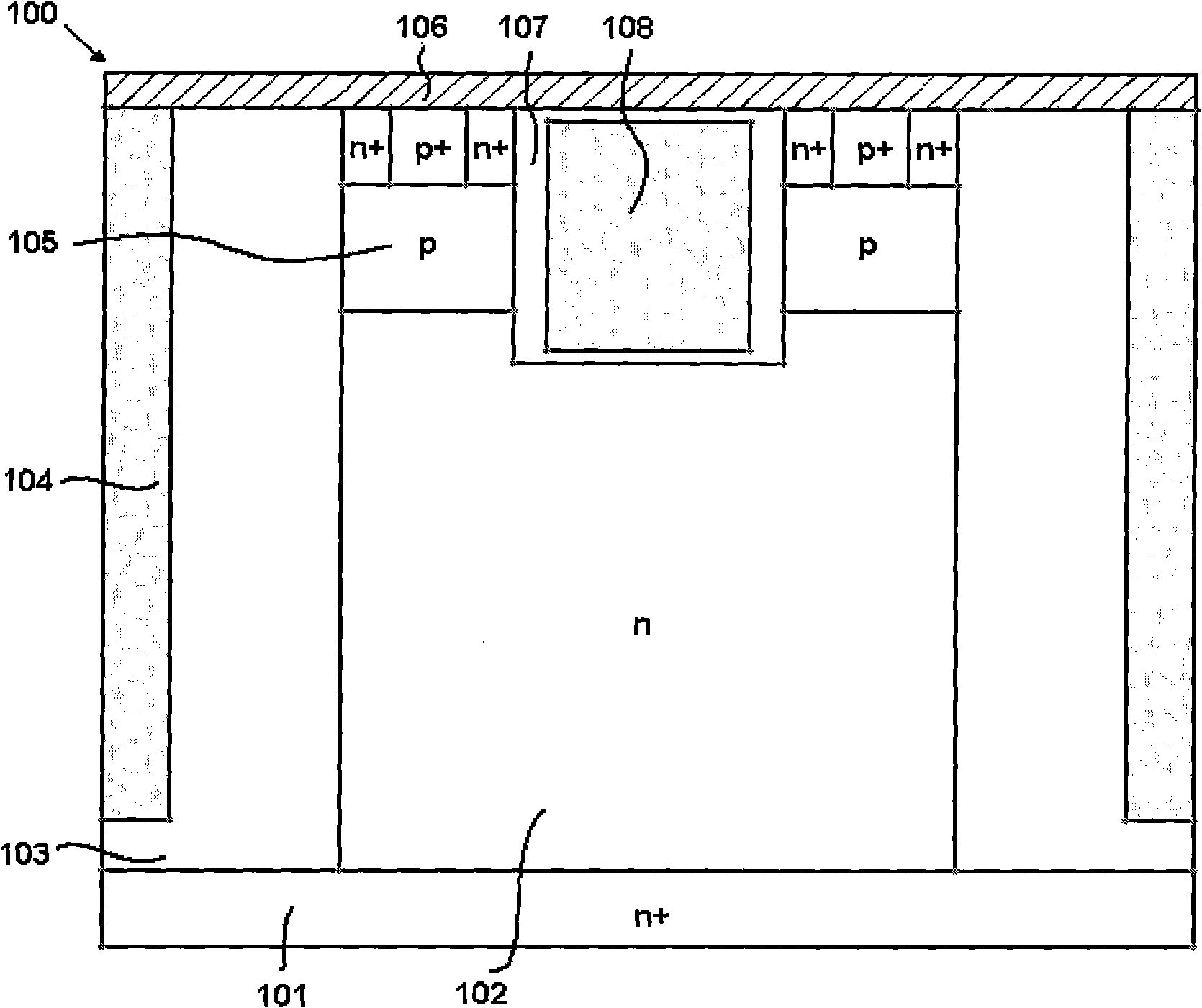
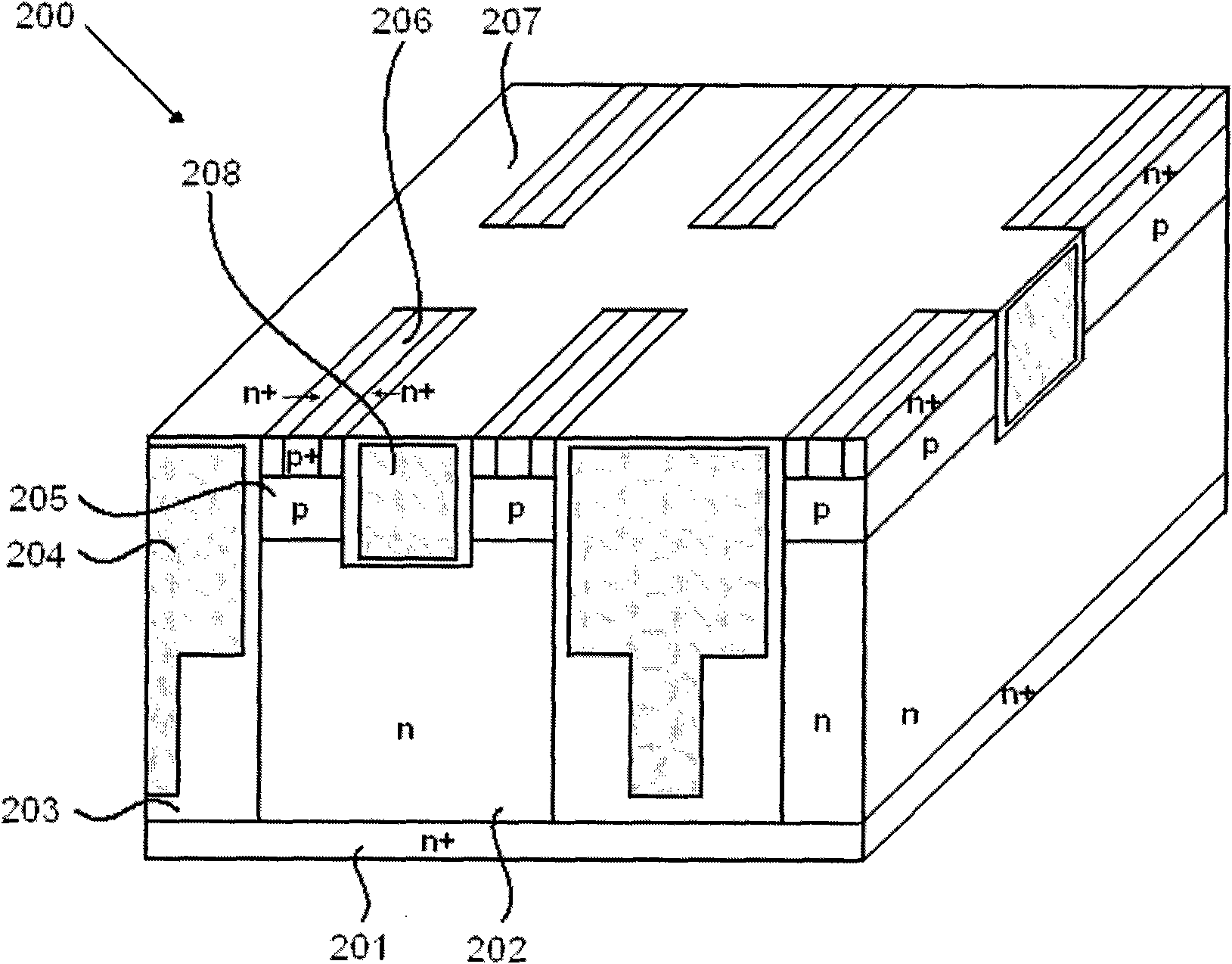
[0015] refer to figure 2 , the modulated on-resistance UMOS transistor of the present invention. It includes a drain region 201 , a drift region 202 , a field oxide layer 203 , a polysilicon plate 204 connected to a gate electrode 208 , a channel region 205 , a source electrode 206 , a gate oxide layer 207 , and a gate electrode 208 . The electrodes of the field plates are shorted to the gate electrodes of the UMOS transistors. According to the requirements of the specific conduction characteristics and breakdown characteristics of the device, determine figure 2 The doping concentration and two-dimensional size of the drift region 202, and the two-dimensional size of the field oxide layer 203.

[0016] When the device of the present invention is turned off in the reverse direction, the side oxygen modulation structure modulates the electric field distribution...


PUM


Abstract

The invention provides a UMOS transistor capable of modulating on resistance, which comprises a drain region (201), a drift region (202), a field oxidation layer (203), a polysilicon polar plate (204), a channel region (205), a source electrode (206), a gate oxidation layer (207) and a gate electrode (208), wherein the polysilicon polar plate (204) is connected with the gate electrode (208). The size of each region of a device can be specifically set according to the requirements on the specific conducting characteristic and the breakdown characteristic of the device. The structure can simultaneously take the requirement of reducing drain-source on resistance into consideration on the premise of not giving up the voltage resistance of the device. The UMOS transistor is compatible with a conventional UMOS transistor process, has strong practicability and is easier to meet the application requirements of a power electronic system.

Description

(1) Technical field [0001] The invention relates to an electronic component, in particular to a trench gate vertical metal oxide semiconductor field effect transistor (UMOSFET), in particular to a modulated on-resistance UMOS transistor. (2) Background technology [0002] In the field of power electronics, power MOSFETs are widely used in switching device structures. In order to make the function of the switching device play well, the power MOSFET needs to meet two requirements: 1. When the device is in the on state, it can have a very low on-resistance to minimize the power loss of the device itself; 2. When the device is in the In the off state, it can have a sufficiently high reverse breakdown voltage. Yung C.Liang proposed a new type of device to replace Super Junction in the low voltage range, called side oxygen modulation (oxide-bypassed, abbreviated as OB) structure device (Y.C.Liang, K.P.Gan and G S.Samudra: IEEE Electron Device Lett. 22(2001) 407). The OB structu...

Claims


Application Information

Patent Timeline
Patent Type & Authority Patents(China)
IPC IPC(8): H01L29/06H01L29/78
Inventor 王颖胡海帆曹菲
Owner 如皋市生产力促进中心
Why Eureka
Try Eureka