Deep slot power semiconductor field effect transistor

A technology of field effect transistors and power semiconductors, applied in semiconductor devices, electrical components, circuits, etc., can solve the problems of no contribution to current conduction, limited device performance, and large area occupied by side oxygen structures, so as to reduce the on-resistance , enhance stability, and increase the effect of drain-source current density

Inactive Publication Date: 2012-01-04
HARBIN ENG UNIV
View PDF0 Cites 0 Cited by
  • Summary
  • Abstract
  • Description
  • Claims
  • Application Information

AI Technical Summary

Problems solved by technology

However, the side oxygen structure of the GOB structure occupies a large area and does not contribute to the current conduction of the device when the device is turned on, which directly limits the performance of the device.

Method used


Image

  • Deep slot power semiconductor field effect transistor
  • Deep slot power semiconductor field effect transistor
  • Deep slot power semiconductor field effect transistor

Examples


Embodiment Construction

[0014] Hereinafter, the present invention will be described in more detail with examples in conjunction with the accompanying drawings:

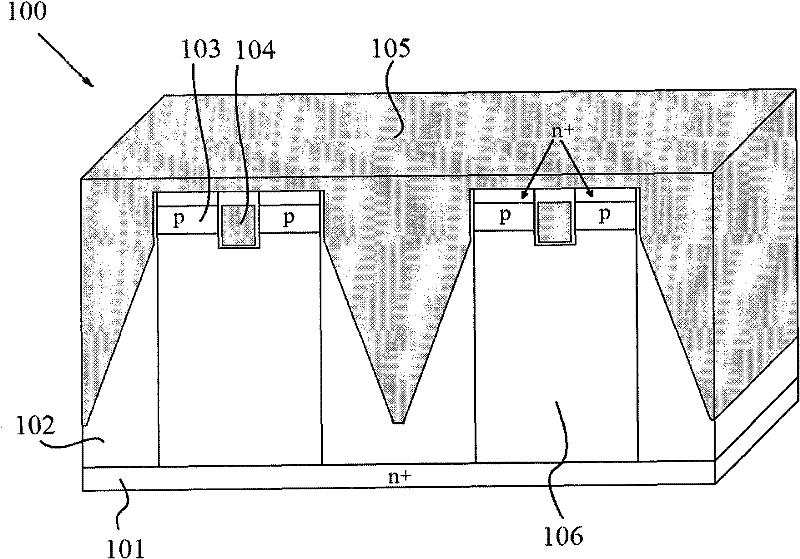
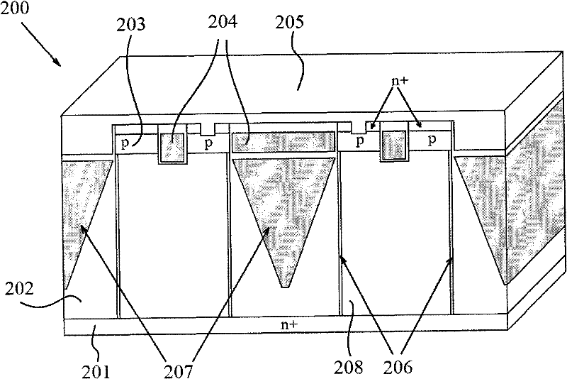
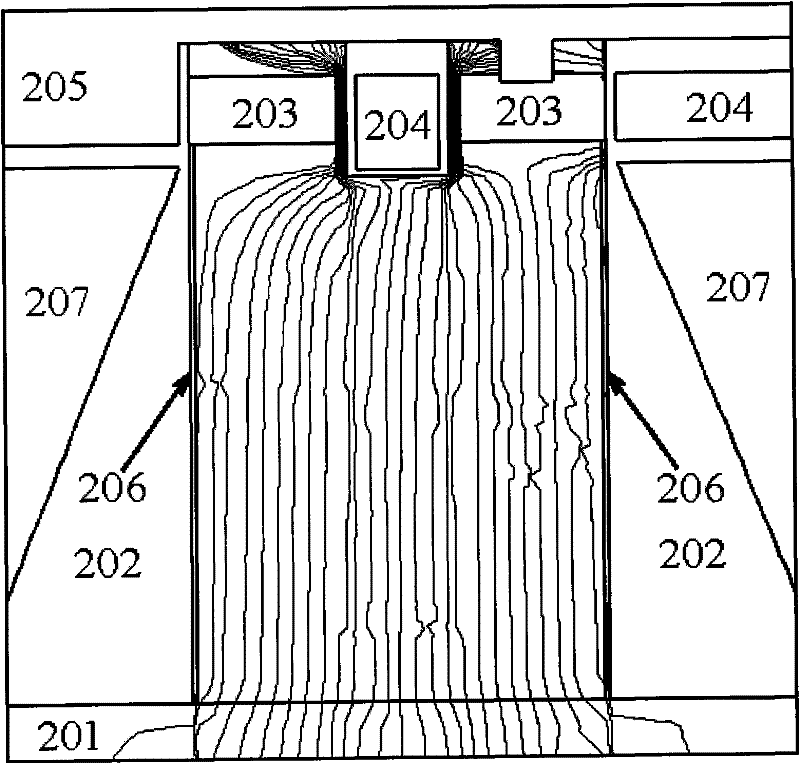
[0015] Reference figure 2 , The deep trench power MOSFET of the present invention. It includes a drain region 201, an oxide layer 202, a channel region 203, a gate electrode 204, a source electrode 205, an n+ layer 206, a split electrode 207, and a drift region 208. It is characterized in that n+ layers are added to both sides of the n-type drift region, and the source electrode 205 and the gate electrode 204 above the split electrode 207 are alternately arranged in the lateral direction. Determine the thickness of the oxide layer 202 between the n+ layer 206, the source electrode 205 and the split electrode 207, the thickness of the oxide layer 202 between the gate electrode 204 and the split electrode 207, according to the specific conduction characteristics and breakdown characteristics of the device. And split electrode 20) and other stru...


PUM


Abstract

The invention provides a deep slot power semiconductor field effect transistor comprising a drain region (201), an oxide layer (201), a channel region (203), a gate electrode (204), a source electrode (205), an n+ numbered layer (206), a splitting electrode (207) and a drift region (208), wherein the drift region is an n-type drift region, two sides of the n-type drift region are provided with ann+layer (206), and the source electrode (205) and the gate electrode (204) above the splitting electrode (207) are alternately arranged breadthwise. The invention adds the n+layer in the n-type driftregion, and the source electrode and the gate electrode above the splitting electrode are alternately arranged breadthwise; on the premise of keeping the resistance to pressure of the device, the invention also gives consideration to the requirement of lowering drain-source conducting resistance. The invention is compatible with common MOSFET technology, has strong actionability and better satisfies the application requirements of power electronic systems.

Description

Technical field [0001] The present invention relates to a vertical metal oxide semiconductor field effect transistor (Vertical MOSFET), in particular to a deep trench power MOSFET. Background technique [0002] In the field of power electronics, power MOSFETs are widely used in switching device structures. In order for the function of the switching device to be played well, the power MOSFET needs to meet two requirements: 1. When the device is in the on state, it can have a very low on-resistance and minimize the power loss of the device itself; 2. When the device is in In the off state, it can have a sufficiently high reverse breakdown voltage. Yung C. Liang proposed a new type of device that replaces Super Junction in the low-voltage range, called Gradient Oxide-Bypassed (GOB) structure device (Yn Chen, Yung C. Liang and GS). Samudra: IEEE Transactions on Power Electronics 22 (4) 2007). The GOB structure converts the impurity concentration matching problem that is difficult ...

Claims


Application Information

Patent Timeline
Patent Type & Authority Patents(China)
IPC IPC(8): H01L29/78H01L29/06H01L29/423
Inventor 王颖胡海帆赵旦峰焦文利
Owner HARBIN ENG UNIV
Why Eureka
Try Eureka