Process for mfg. multi-phase diffraction optic element

A technology of diffractive optical elements and phases, which is applied in the fields of optical elements, pattern surface photolithography, optics, etc. It can solve the problems that it is difficult to ensure the accuracy of overlay, the accuracy of overlay is difficult to guarantee, and the device efficiency is difficult to exceed 90%.

Inactive Publication Date: 2003-03-12
HUAZHONG UNIV OF SCI & TECH
View PDF0 Cites 22 Cited by
  • Summary
  • Abstract
  • Description
  • Claims
  • Application Information

AI Technical Summary

Problems solved by technology

In the existing manufacturing process of diffractive optical elements, as the number of steps increases, the pattern structure of the reticle becomes finer and more difficult to guarantee the accuracy of overlay. Therefore, when the numbe

Method used


Image

  • Process for mfg. multi-phase diffraction optic element
  • Process for mfg. multi-phase diffraction optic element
  • Process for mfg. multi-phase diffraction optic element

Examples


Embodiment Construction

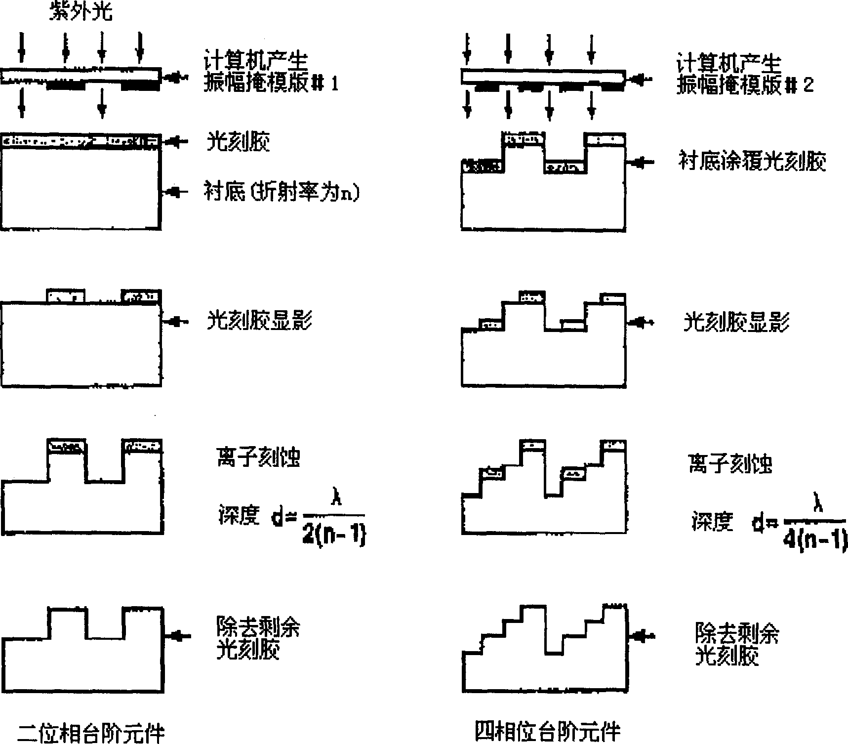
[0020] figure 2 It shows the specific process implementation process of making 8-phase diffractive microlens array by using the self-alignment process of the invention.

[0021] ①Sputter a 0.8μm thick chromium film on the substrate to be made into a microlens by a magnetron sputtering apparatus, then throw a positive photoresist, and after pre-baking, use the first mask to expose, such as figure 2 (a);

[0022] ②After developing and hardening the film, wet-etch the chromium film not masked by the glue, and use reactive ion beam etching (RIE) technology to etch the substrate with a depth of d / 8, where d is the total etching phase depth, such as figure 2 (b). At this time, an initial distribution of 8-phase steps is formed, and the subsequent process does not require strict alignment of the dark and bright boundaries of the mask with the boundaries of these steps.

[0023] ③Continue to shake the positive photoresist and expose it with the second mask, such as figure 2 As...


PUM


Abstract

A process for preparing multi-phase optical diffraction element includes sputtering Cr film on substrate, exposing the nagative photoresist on the back to form mask, determining the positions of each steps, etching ultraviolet transmitting substance (SiO2) with reactive ions, etc. Its advantages are low precision requirement of masks except the first one, and high diffraction efficiency.

Description

technical field [0001] The invention belongs to the field of information science and technology, and specifically relates to a process for manufacturing a multi-phase diffractive optical element. Background technique [0002] Binary optics, or binary diffractive optics, was first proposed abroad by Veldcamp et al. at the Massachusetts Institute of Technology (MIT) in the late 1980s. The control of the phase in the binary optical element is to approach the ideal value by generating multiple steps. For example, the phase step is 2π, you can press L=2, 4, 8,..., 2 m , (m is a positive integer) equal division method to divide, this method is geometrically equivalent to the surface of any shape can be approached by multi-step plane. In the existing manufacturing process, this binary phase step is easily completed by microelectronics technology: a simple black and white mask can be exposed and etched to produce two levels of steps, such as another mask, repeated exposure And et...

Claims


Application Information

Patent Timeline
IPC IPC(8): G02B5/00G02B27/42G03F7/00
Inventor 陈四海李毅赖建军何苗易新建
Owner HUAZHONG UNIV OF SCI & TECH
Why Eureka
Try Eureka