Semiconductor momory

A storage device and semiconductor technology, applied in the fields of semiconductor devices, information storage, semiconductor/solid-state device manufacturing, etc., can solve the problems of not finding a solution to shorten the length of the bit line wiring, shrinking the 2-port SRAM cell, etc.

Inactive Publication Date: 2003-05-21
MITSUBISHI ELECTRIC CORP
View PDF3 Cites 6 Cited by
  • Summary
  • Abstract
  • Description
  • Claims
  • Application Information

AI Technical Summary

Problems solved by technology

In addition, although the "memory cell" disclosed in the above-mentioned Japanese Unexamined Publication No. 07-7-89 is a design scheme of a 2-port SRAM unit, what is provided is that there is no major change to the design scheme of a single-port SRAM unit and can be easily The design scheme of adding the second port is not to shrink the 2-port SRAM cell in the direction of the bit line
[0019] Similarly, low power consumption type SRAM memory cells such as low power consumption type SRAM memory cells such as SRAM memory cells with a low power consumption type 8 transistor structure that will be shrunk to the flow selection signal line in the column direction from the memory cell selected by the word line as the row selection signal line have not been found. A specific solution to shorten the wiring length of the bit line

Method used


Image

  • Semiconductor momory
  • Semiconductor momory
  • Semiconductor momory

Examples


Embodiment 1

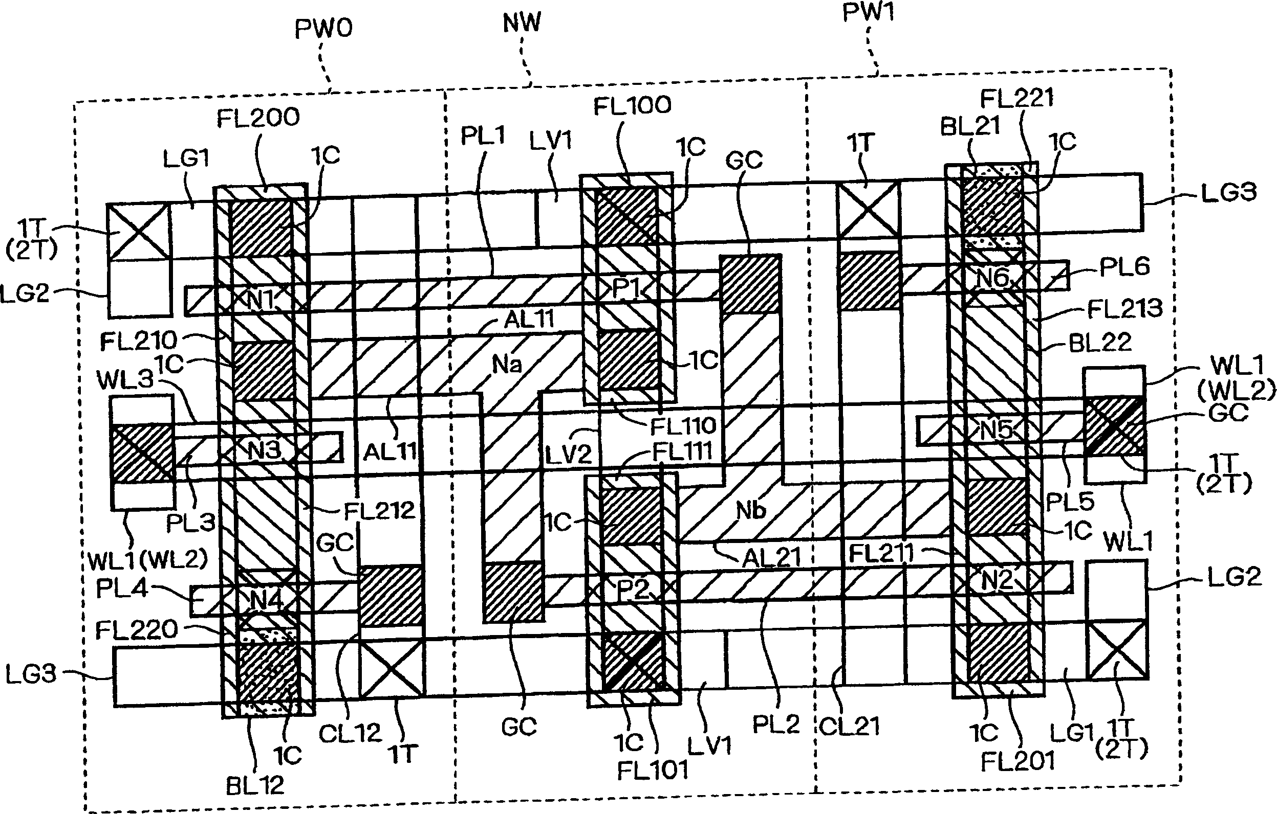
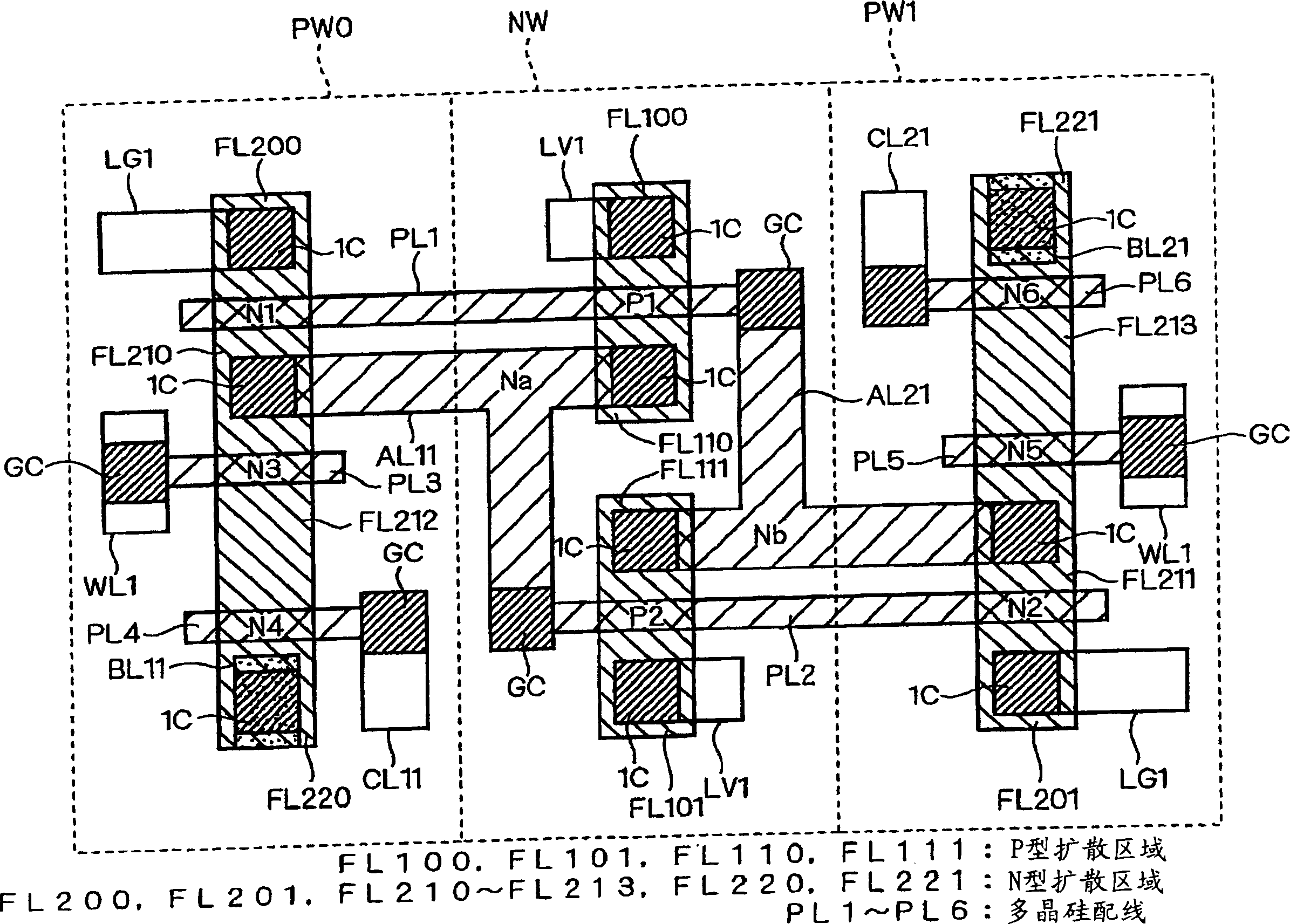
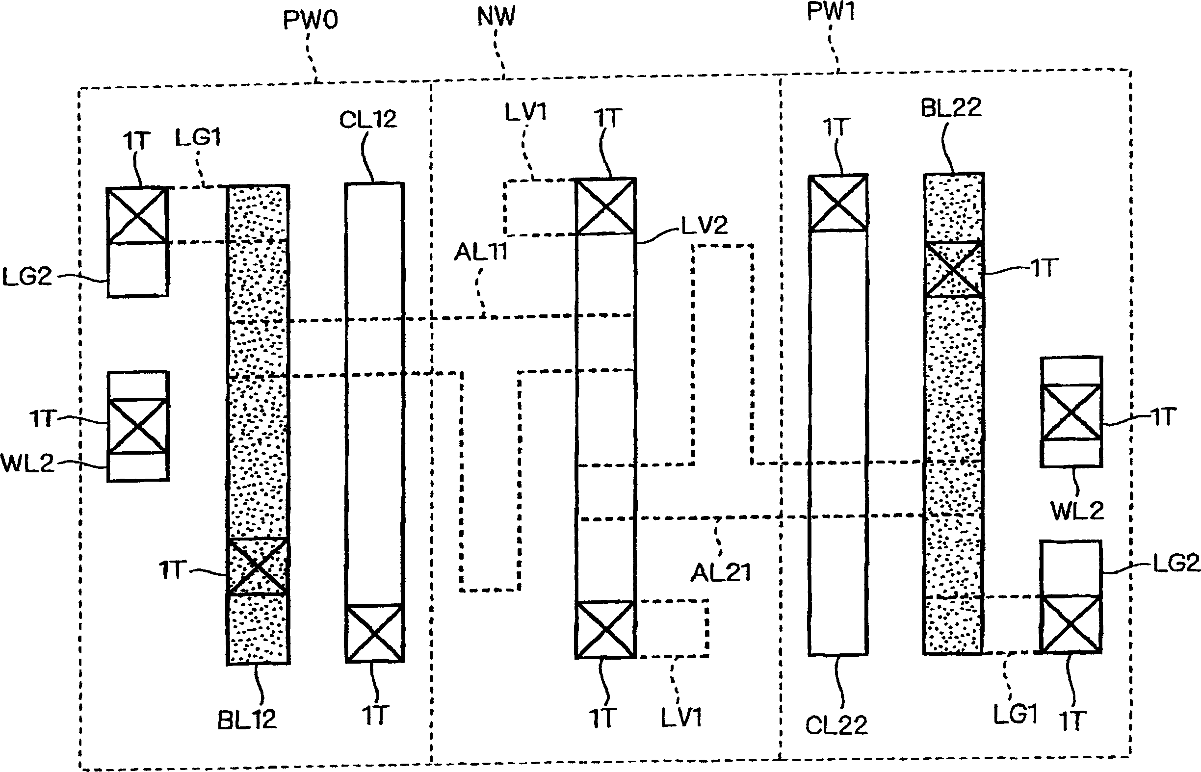
[0060] figure 1 It is an explanatory diagram showing the design structure on the entire layer of the memory cell of the SRAM according to the first embodiment of the present invention. figure 2 is the main expression figure 1 An explanatory diagram of the design structure under the 1st aluminum wiring layer. image 3 is the main expression figure 1 An explanatory diagram of the design structure of the second aluminum wiring layer. Figure 4 is the main expression figure 1 An explanatory diagram of the design structure of the third aluminum wiring layer. which is, Figure 2 ~ Figure 4 is for easy understanding figure 1 The design scheme structure shown is divided into each wiring layer shown in the figure 1 Supplementary Fig. Figure 5 yes means Figure 1 ~ Figure 4 A circuit diagram of an equivalent circuit of the memory cell of Embodiment 1 shown. exist figure 1 in, sometimes omitted Figure 2 ~ Figure 4 Part of the symbol shown.

[0061] Such as Figure...

Embodiment 2

[0099] Figure 6 It is an explanatory diagram showing the design structure on the entire layer of the memory cell of the SRAM according to the second embodiment of the present invention. Figure 7 is the main expression Figure 6 An explanatory diagram of the design structure under the 1st aluminum wiring layer. Figure 8 is the main expression Figure 6 An explanatory diagram of the design structure of the second aluminum wiring layer. which is, Figure 7 and Figure 8 for easy understanding Figure 6 The design scheme structure shown is divided into each wiring layer shown in the Figure 6 Supplementary Fig. exist Figure 6 in, sometimes omitted Figure 7 and Figure 8 Part of the symbol shown. in addition, Figure 6 ~ Figure 8 The equivalent circuit diagram of the memory cell shown in Embodiment 2 and Figure 5 Example 1 shown is the same.

[0100] Next, differences from Embodiment 1 will be described. Such as Figure 6 ~ Figure 8 As shown, the NMOS transist...

Embodiment 3

[0105] Figure 9 It is an explanatory diagram showing the design structure on the entire layer of the memory cell of the SRAM according to the third embodiment of the present invention. Figure 10 is the main expression Figure 9 An explanatory diagram of the design structure under the 1st aluminum wiring layer. Figure 11 is the main expression Figure 9 An explanatory diagram of the design structure of the second aluminum wiring layer. which is, Figure 10 return Figure 11 is for easy understanding Figure 9 The design scheme structure shown is divided into each wiring layer shown in the Figure 9 Supplementary Fig. exist Figure 9 in, sometimes omitted Figure 10 and Figure 11 Part of the symbol shown. in addition, Figure 9 ~ Figure 11 The equivalent circuit diagram of the memory cell shown in Embodiment 3 and Figure 5 Example 1 shown is the same.

[0106] Next, differences from Embodiment 2 will be described. N-type diffusion region FL210 is electrically...


PUM


Abstract

A semiconductor storage apparatus having an SRAM memory cell of a low power consumption type which can reduce a wiring length of a bit line. NMOS transistors N1, N3 and N4 are formed in a P well region PW0, NMOS transistors N2, N5 and N6 are formed in a P well region PW1 and a wiring direction (a second direction) of bit lines BL1 and BL2 (bit lines BL12 and BL22) is set to be orthogonal to a direction of separation arrangement (a transverse direction in the drawing; a first direction) of the P well regions PW0 and PW1. The P well region PW0 and the P well region PW1 are formed opposite to each other with an N well region interposed therebetween.

Description

technical field [0001] The present invention relates to a memory cell structure of a semiconductor memory device having a SRAM (Static RAM) memory cell. Background technique [0002] In recent years, with the lightness, thinness, and miniaturization of electronic instruments, it is strongly required to realize the functions of these devices at high speed. It is indispensable to mount a microcomputer in such an electronic device, and it is necessary to incorporate a large-capacity and high-speed memory in the structure of the microcomputer. In addition, in addition to the rapid spread and high performance of computers, in order to realize higher-speed processing, it is required to increase the capacity of the cache memory. That is, RAM used when the CPU executes a control program or the like is required to be rigid and increase in capacity. [0003] As RAM, DRAM (Dynamic RAM) and SRAM are generally used, and SRAM is generally used for a part requiring high-speed processing ...

Claims


Application Information

Patent Timeline
Patent Type & Authority Applications(China)
IPC IPC(8): G11C11/41G11C11/412H01L21/8244H01L27/11
CPCG11C11/412H10B10/00
Inventor 新居浩二
Owner MITSUBISHI ELECTRIC CORP
Why Eureka
Try Eureka