Electric charge pump with wide output voltage area
An output voltage, charge pump technology, applied in electrical components, regulating electrical variables, automatic power control, etc., can solve the problems of current replication errors, not considering the current adaptability of positive current sources and negative current sources, etc.
- Summary
- Abstract
- Description
- Claims
- Application Information
AI Technical Summary
Problems solved by technology
Method used
Image
Examples
Embodiment Construction
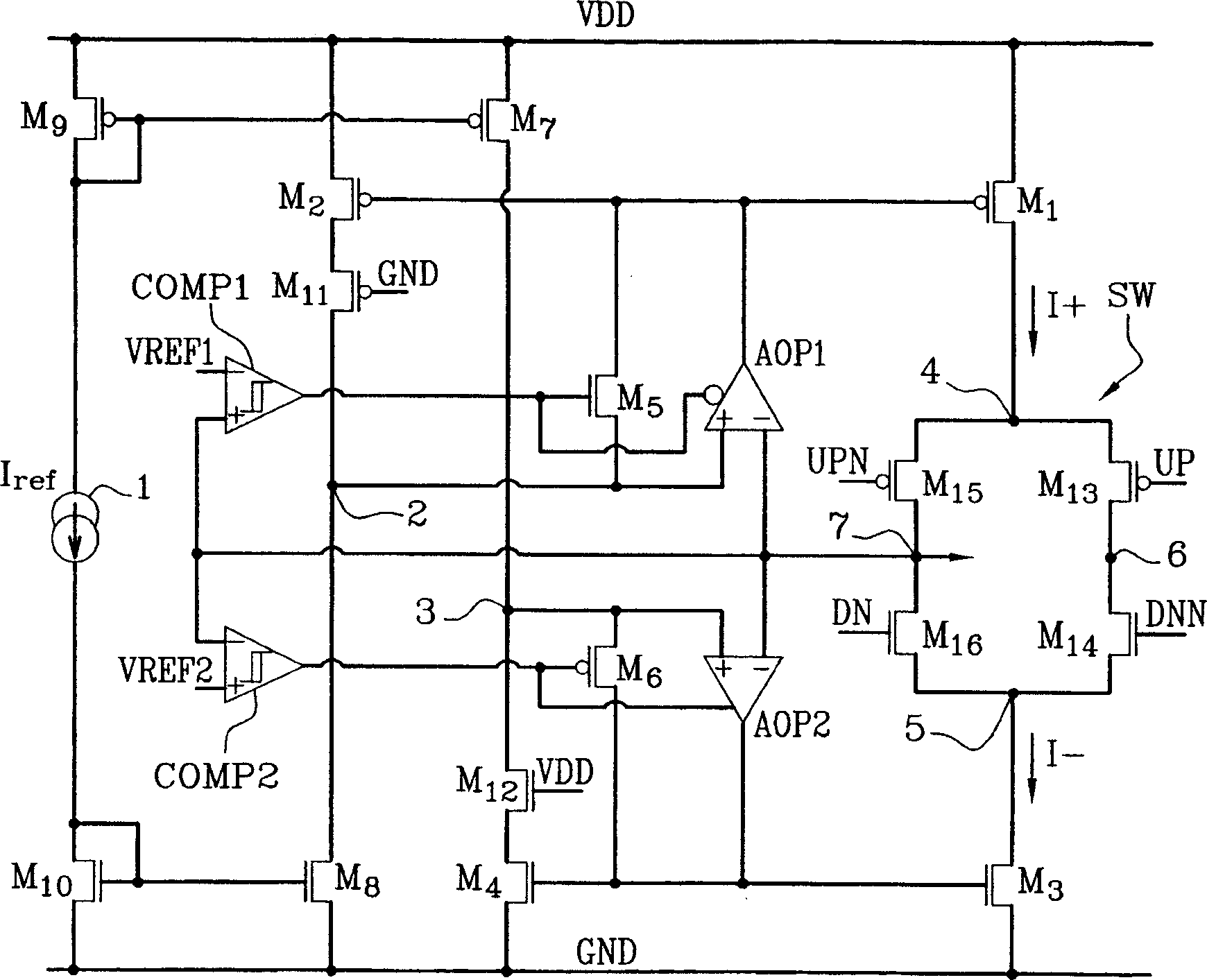
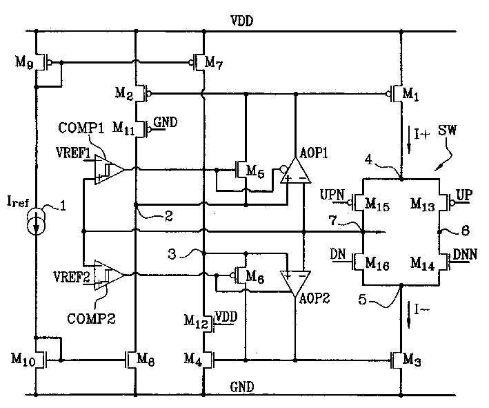
[0022] figure 1 shows a charge pump according to the invention, wherein a charge pump at a supply voltage V is shown in particular detail DD Bipolar current source between ground and GND. This bidirectional current source that constitutes the charge pump is implemented in accordance with CMOS (abbreviation for "Complementary Metal Oxyde Semieonductor" in English-Saxon) technology.
[0023] There is a first branch in the charge pump mentioned above, which is composed of a diode-connected P-type MOS transistor M9, a current source 1 generating a reference current Iref, and a diode-connected N-type MOS transistor M10 in series.
[0024] The second branch in the charge pump is formed in series by the first MOS transistor M8, the second MOS transistor M11, the node 2 between them, and the third current duplication MOS transistor M2. Transistor M2 forms a mirror image with MOS transistor M1 constituting a positive current source.
[0025] The source of the transistor M8 is then g...
PUM
 Abstract
Description
Claims
Application Information

