Computer-aided technique planning method for silicon micro-component

A computer-aided and process planning technology, applied in computing, instruments, special data processing applications, etc., can solve problems such as lack of intuition, high requirements for designers’ process knowledge, and no systematic summary of 3D manufacturing characteristics of micro devices. Achieve fewer iterations, fewer counts, fewer etch and photolithography steps

Inactive Publication Date: 2003-10-15
XI AN JIAOTONG UNIV
View PDF0 Cites 16 Cited by
  • Summary
  • Abstract
  • Description
  • Claims
  • Application Information

AI Technical Summary

Problems solved by technology

[0009] 1) Most of the CAD systems used for MEMS are aimed at the "forward" design process, and the micro-process planning modules included rarely involve the automatic generation of the process, but only edit the process, which req

Method used


Image

  • Computer-aided technique planning method for silicon micro-component
  • Computer-aided technique planning method for silicon micro-component
  • Computer-aided technique planning method for silicon micro-component

Examples


Example Embodiment

[0033] In order to understand the present invention more clearly, the present invention will be further described in detail below in conjunction with the accompanying drawings and the examples completed by the inventor according to the technical solution of the present invention. 5. Contents of the invention

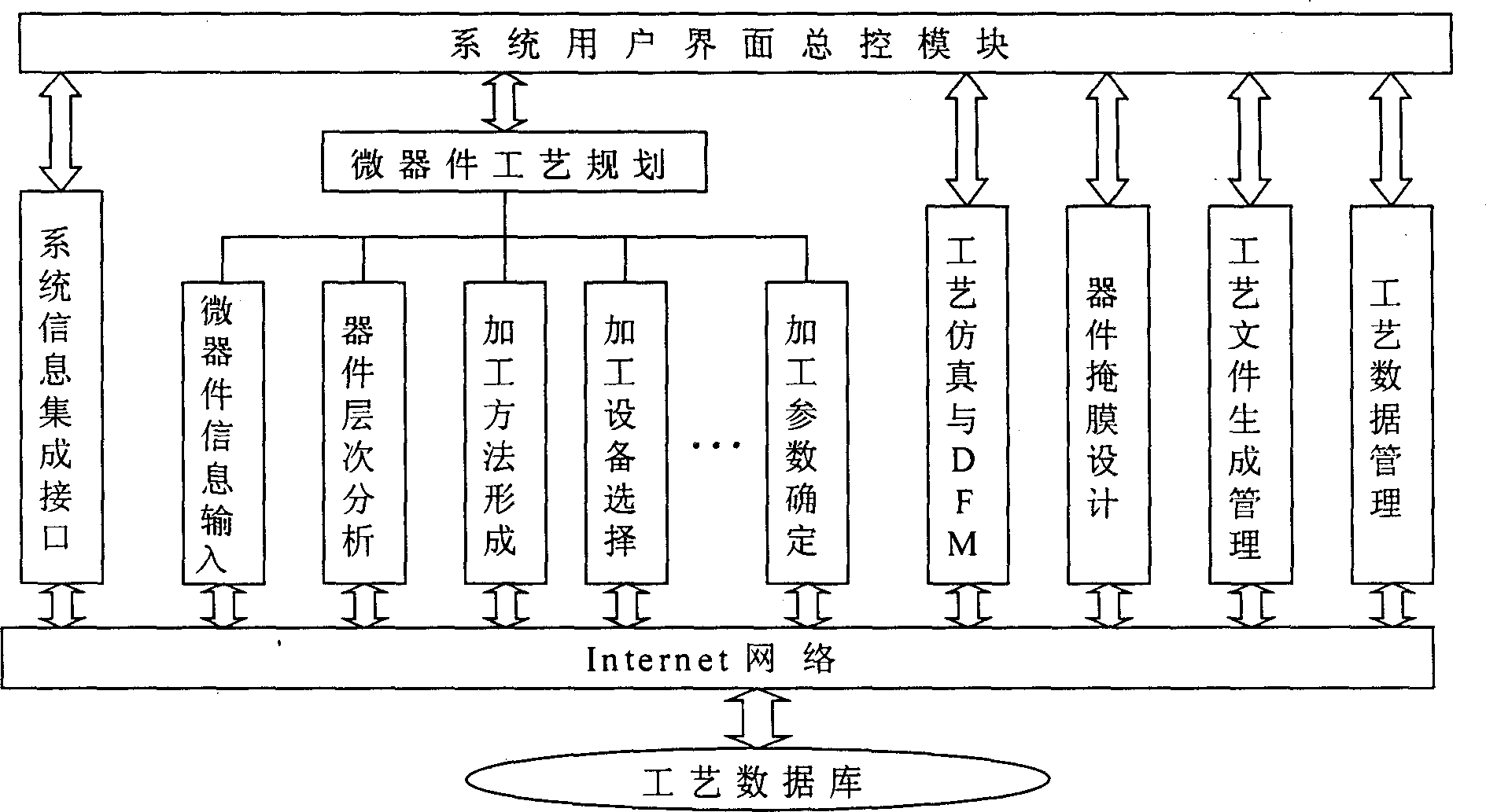
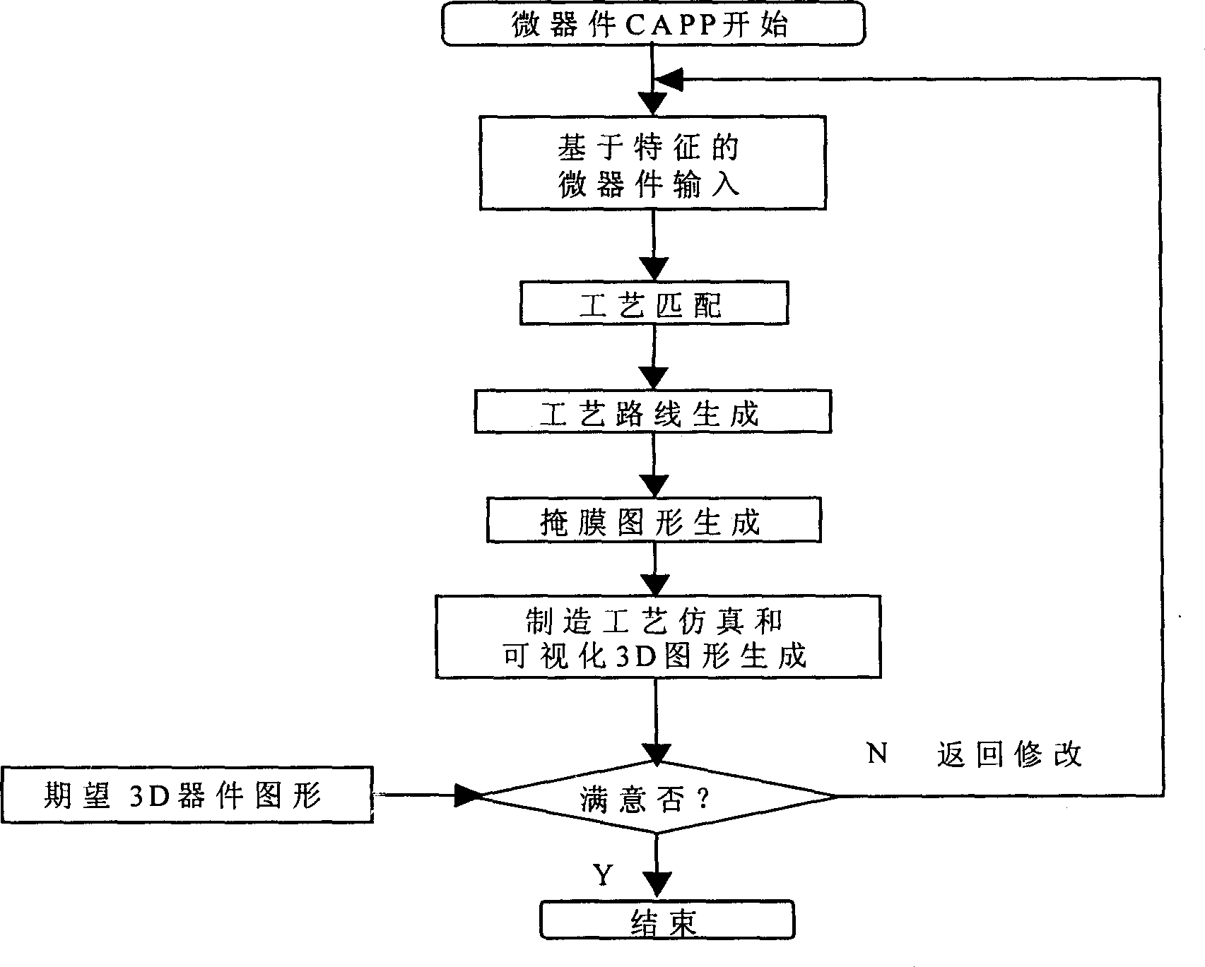
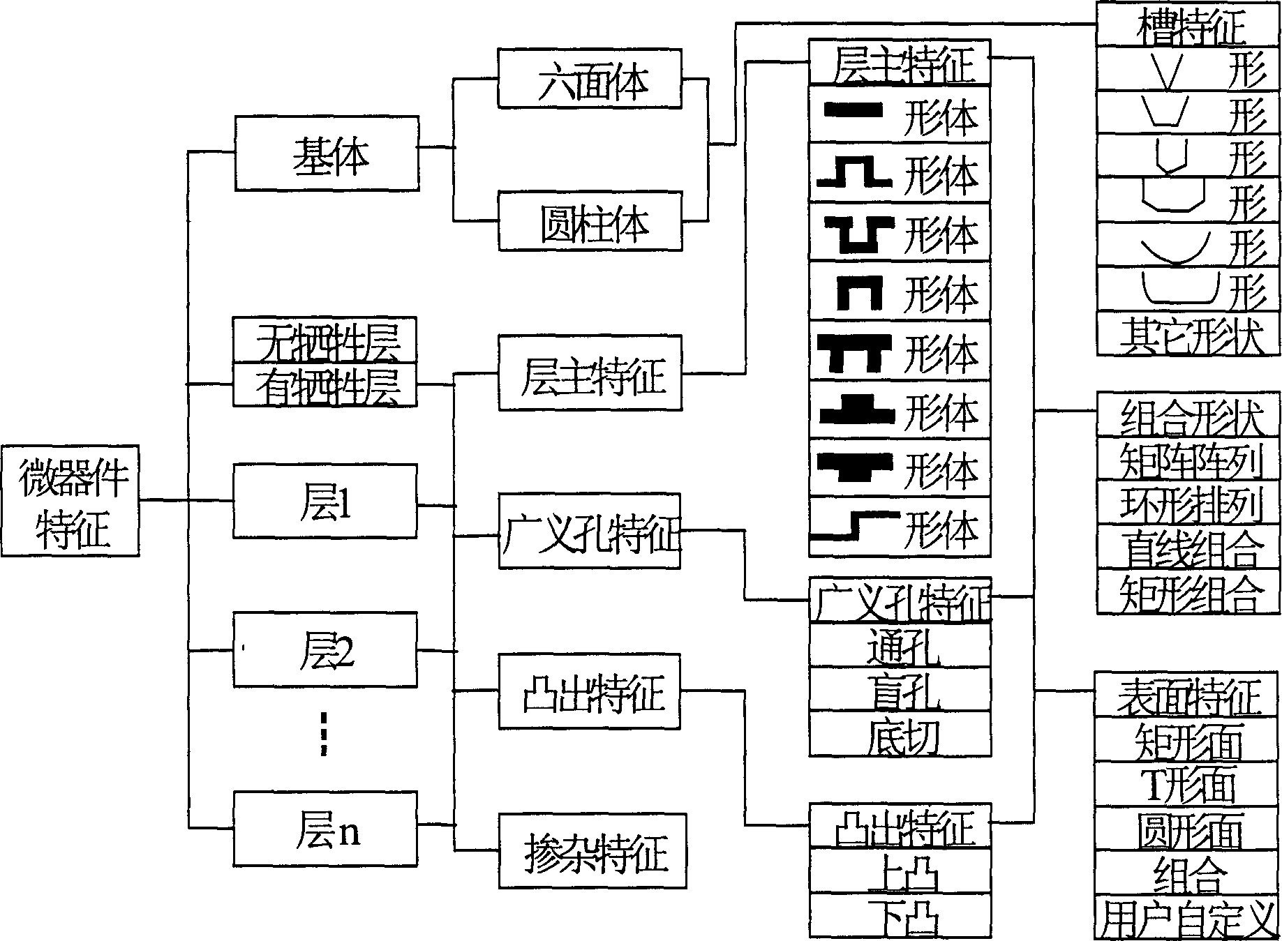
[0034] The method of the present invention is to decompose the three-dimensional geometric structure of the micro-device according to the processing layer, each layer is composed of layer main features and several auxiliary features, and a complete three-dimensional and two-dimensional surface manufacturing feature of the micro-device is established. The micromachining method is linked and reflects the constraints of the micromachining process. The relationship between MEMS layout and mask and micromachining process design is established. With a given 3D micro-device model, the system merges the main features of the micro-device hierarchically, reducing the number of pr...


PUM


Abstract

The present invention discloses the computer-aided technological planning method with stereo micro processing and surface micro processing as research object. The 3D geometrical structure of micro device is decomposed into several processing layers comprising main characteristic and auxiliary characteristics, and complete 3D and 2D manufacture characteristics of micro device are established with the manufacture characteristics being associated with the silicon-based micro processing method and reflecting the constraint condition of the micro processing. The relationship between MEMS layout and the mask and micro processing design is established. Via the three-dimensional micro device model, the numbers of processing steps and masks are decreased via the layer merging. The relationship between characteristic indexing tree and characteristics is formed and various models are established in technological process and mask pattern design. Technological data and CIF format mask files are finally created.

Description

[0001] 1. The technical field mentioned [0002] The invention belongs to the field of computer application technology. It involves the basic theory, software development methods, related algorithms and programming implementation methods for micro-electromechanical system process planning, especially a computer-aided process planning method for silicon-based micro-devices in the "reverse" design process of MEMS. 2. Background technology [0003] The emergence of the MEMS-CAD system has made the related design process get strong support from the computer. At present, many CAD softwares have been developed at home and abroad, such as MIT's MEMCAD (now CoventorWareCAD system), which can simulate the whole process of design and manufacture, including packaging and system-level simulation. IntelliSense's InteliCAD is mainly for electromechanical and thermal analysis, and has greater flexibility in process simulation. NODAS of Carnegie-Mellon University in the United States can qu...

Claims


Application Information

Patent Timeline
IPC IPC(8): G06F17/50
Inventor 江平宇汪继亮刘崢
Owner XI AN JIAOTONG UNIV
Why Eureka
Try Eureka