

High speed simulation method of ion implantation including dose effect
An ion implantation, high-speed simulation technology, applied in semiconductor/solid-state device testing/measurement, discharge tubes, electrical components, etc., can solve problems such as reducing simulation efficiency and prolonging simulation time
- Summary
- Abstract
- Description
- Claims
- Application Information
AI Technical Summary
Problems solved by technology
Method used
Image

Examples
Embodiment Construction
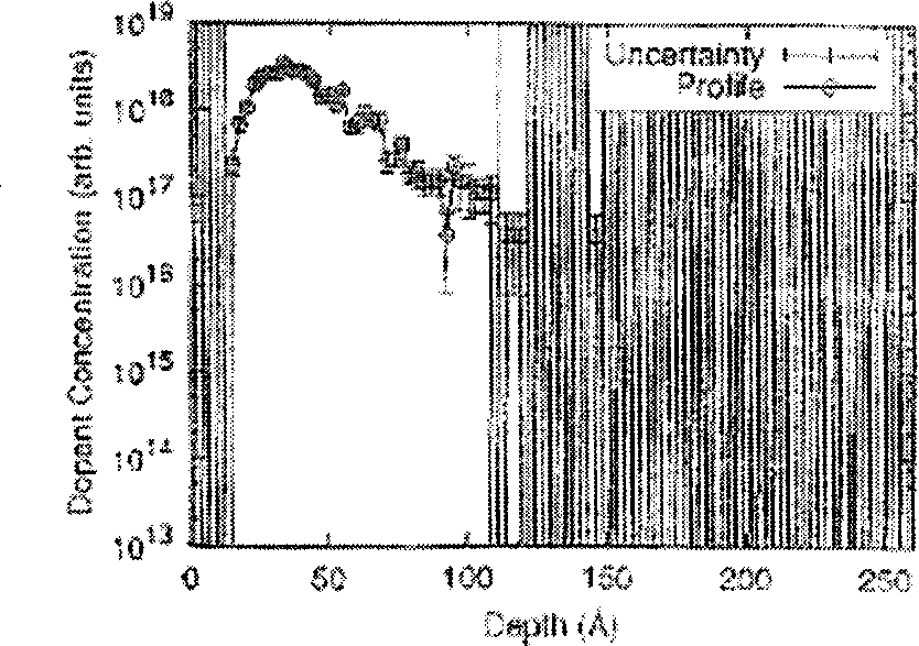
[0032] The following gives the simulation of arsenic 80keV energy, 1e13cm using the SMDE method -2 The specific process of dosage implantation of crystalline silicon:
[0033] 1. Determine the size S of the injection window in the simulation, usually 20a×20a, a is the side length of the crystal lattice of crystalline silicon, about 5.432 angstroms, then the size of S is 11802.6496 square angstroms.
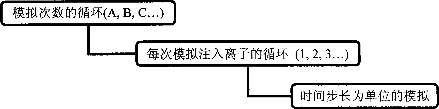
[0034] 2. The injection dose is 1e13 (unit is cm -2 ) and the simulation window size S determine the number N of implanted ions simulated in one simulation experiment, N=D×S, and the number of implanted ions simulated in one simulation experiment is 118 ions.
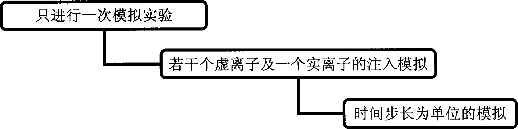
[0035] 3. Set the depth position of each split layer, select the number of split layers as 9, and then mark each split layer as d 1 , d 2 , d 3 ,...,d 9 . During the simulation process, when the virtual ion reaches the depth of the splitting layer, splitting occurs, and one virtual ion splits into i virtual ions (here...
PUM
 Abstract
Description
Claims
Application Information