Shift register device and display device

A shift register, phase technology, applied in static memory, digital memory information, instruments, etc., can solve problems such as shift register malfunction

Inactive Publication Date: 2003-11-19
ONANOVICH GROUP
View PDF0 Cites 20 Cited by
  • Summary
  • Abstract
  • Description
  • Claims
  • Application Information

AI Technical Summary

Problems solved by technology

However, when the degradation problem of other transistors constituting the shift register is greatly improved, the degradation of the pull-down element becom

Method used


Image

  • Shift register device and display device
  • Shift register device and display device
  • Shift register device and display device

Examples


Embodiment 1

[0028] Refer to the following Figure 1 to Figure 3 Example 1 of the present invention will be described.

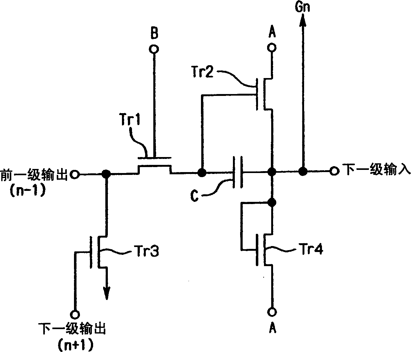
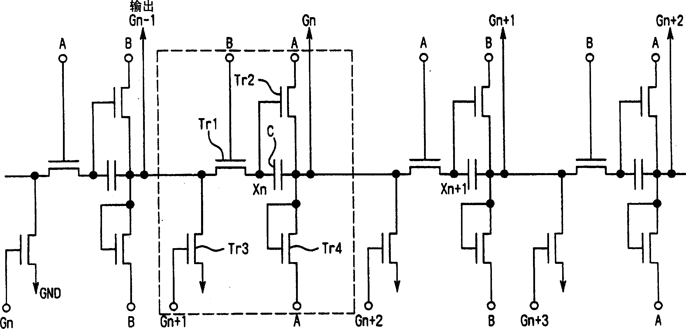
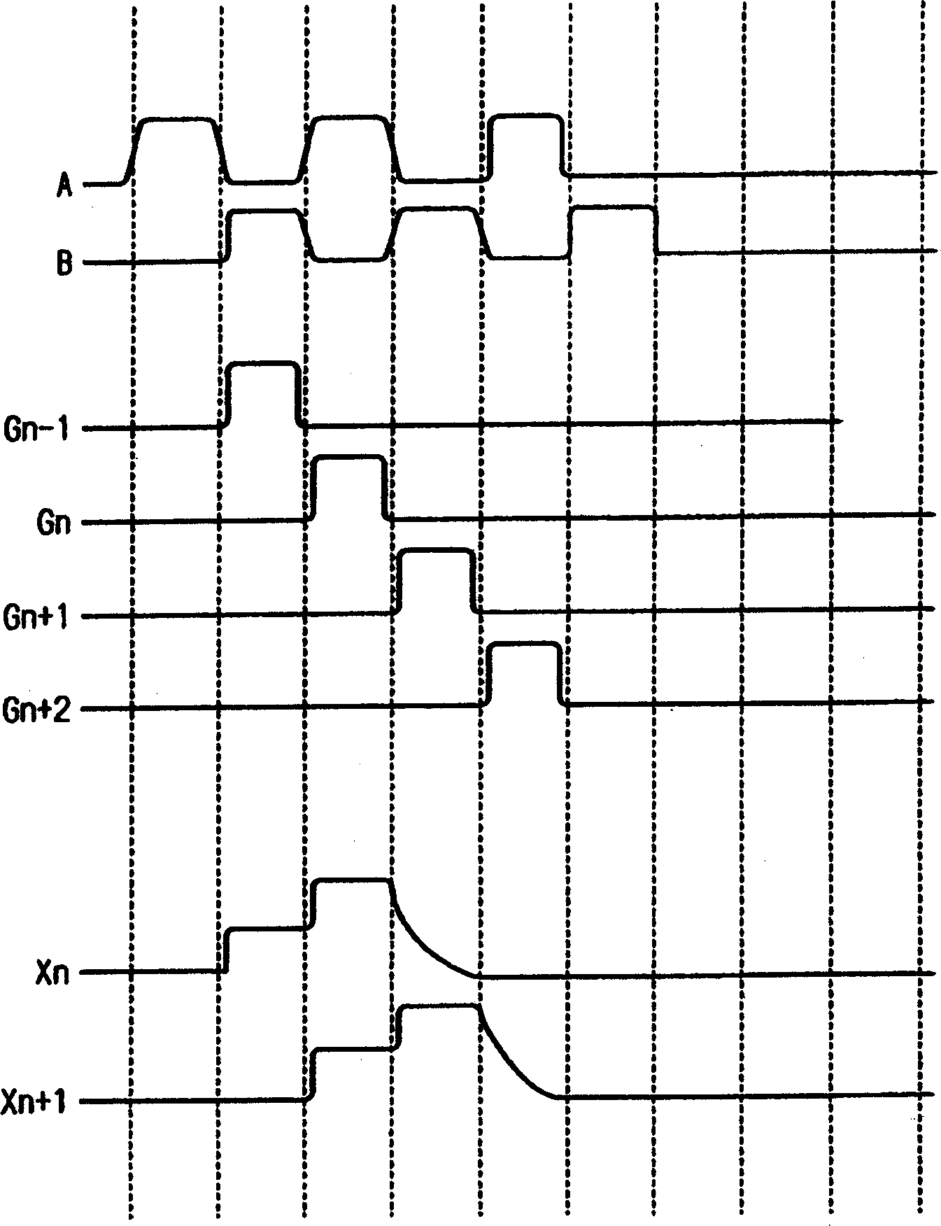
[0029] Figure 1 to Figure 3 is a diagram for explaining the shift register device of this embodiment. This shift register device is composed of a device for generating a plurality of clock signals with sequentially different phases, particularly two-phase clock signals with different phases in this embodiment, and a plurality of cascade-connected stage circuits. in, figure 1 is a circuit configuration diagram of a stage, figure 2 It is a circuit configuration diagram of four stages connected in cascade. image 3 It is a timing chart showing clock signals A, B, output signals Gn-1 to Gn+2, waveform Xn of n-stage control signals, and waveform Xn+1 of n+1-stage control signals.

[0030] Such as figure 1 As shown, each stage circuit is composed of four transistors Tr1~Tr4 and a capacitor C. The input transistor Tr1 is connected to the output of the previous stage,...

Embodiment 2

[0039] Next, an example of a shift register device having a structure in which a plurality of stages are divided into a plurality of modules and a clock signal is sequentially supplied in units of modules will be described. Figure 4 It is a schematic configuration diagram showing the shift register device of this embodiment, and shows an example in which four stages are divided into m modules. Figure 5 is its timing diagram. Since the specific configuration in each stage is the same as that of Embodiment 1, its description is omitted.

[0040] In this embodiment, when the clock control circuit M is driving other modules, all the clock signals of the module are at 'Low' level. That is, if Figure 5 As shown, during the stages S1-S4 of the drive module B1, on the module B1, as described in Embodiment 1, the clock signals A and B are input as the clock signal CK11, while all other modules B2-Bm are 'Low The 'level signals are input as clock signals CKI1 to CKIm.

[0041] Ac...


PUM


Abstract

The invention provides a shift register capable of reducing deterioration of component without easily causing incorrect action due to noise interference. The shift register of the invention includes a generator for generating a plurality of clock signals having different phases, and a plurality of cascaded stages, each generating an output signal. Besides, each stage has an input transistor Tr1, an output transistor Tr2, a clamping transistor Tr3 and a pull-down transistor Tr4. The pull-down transistor Tr4 is a diode-connected transistor, to which the same clock signal as the clock signal input to the output transistor Tr2 is input.

Description

technical field [0001] The present invention relates to a shift register device for supplying scanning signals provided in a display device such as a liquid crystal display device, and a display device including the shift register device. Background technique [0002] For example, in an active-matrix liquid crystal display device, image signal lines (source lines) and scanning signal lines (gate lines) are arranged in a grid pattern, and a thin film for driving liquid crystal of each pixel is provided at the intersection of these lines. Switching elements such as transistors. On a plurality of scanning signal lines, by sequentially scanning these signal lines, all the switching elements on one scanning signal line are in a momentary conduction state, on the other hand, synchronously with the scanning, a plurality of image signals are transmitted. The line provides the image signal. [0003] In this case, it is a shift register that sequentially supplies scanning signals to...

Claims


Application Information

Patent Timeline
IPC IPC(8): G11C19/00G09G3/20G09G3/36
CPCG09G2320/02G09G3/3677G09G3/36
Inventor 蛇口广行
Owner ONANOVICH GROUP
Why Eureka
Try Eureka