
Nitride based semiconductor laser element and method for fabricating the same

A laser device and semiconductor technology, applied in the field of working voltage, can solve problems such as difficulty in improving yield, complicated process, and difficulty in forming a thick insulating layer

Inactive Publication Date: 2003-11-19
SONY CORP
View PDF2 Cites 10 Cited by
  • Summary
  • Abstract
  • Description
  • Claims
  • Application Information

AI Technical Summary

Problems solved by technology

[0011] The third problem is that the process formed based on the stacked structure of the GaN-based epitaxial growth layer is complicated and includes many steps, so it is difficult to increase the yield
In this case, the top surface of the second contact layer, which is the contact surface with the second electrode, may be contaminated
Moreover, a problem is involved here that it is difficult to form a thick insulating layer on both sides of the upper layer of the second cladding layer having a ridge structure.

Method used


Image

  • Nitride based semiconductor laser element and method for fabricating the same
  • Nitride based semiconductor laser element and method for fabricating the same
  • Nitride based semiconductor laser element and method for fabricating the same

Examples


example 1

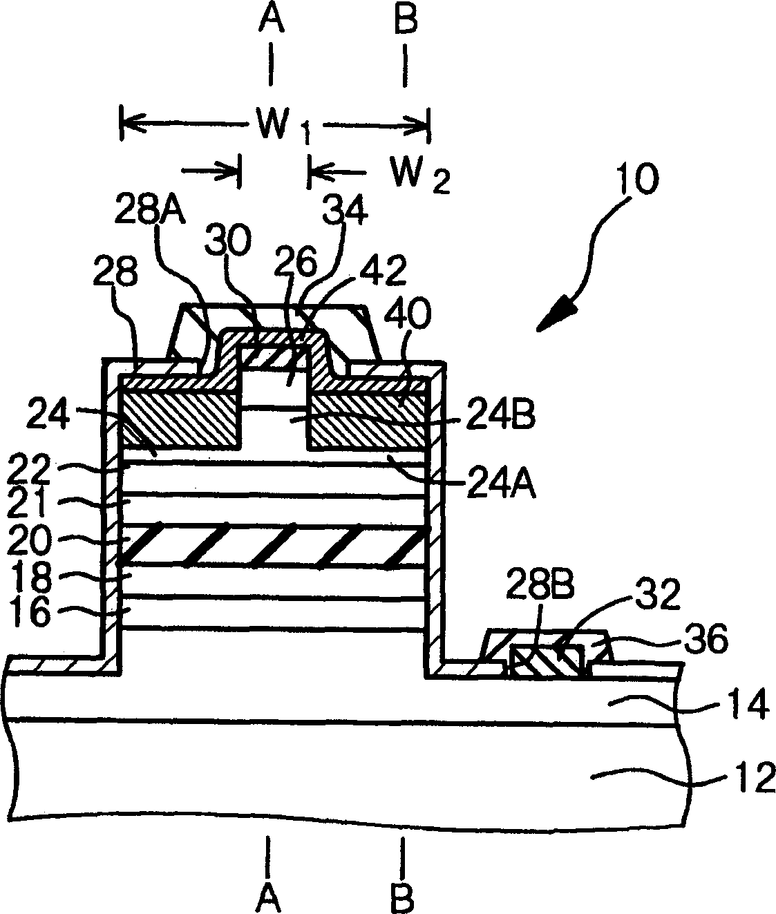
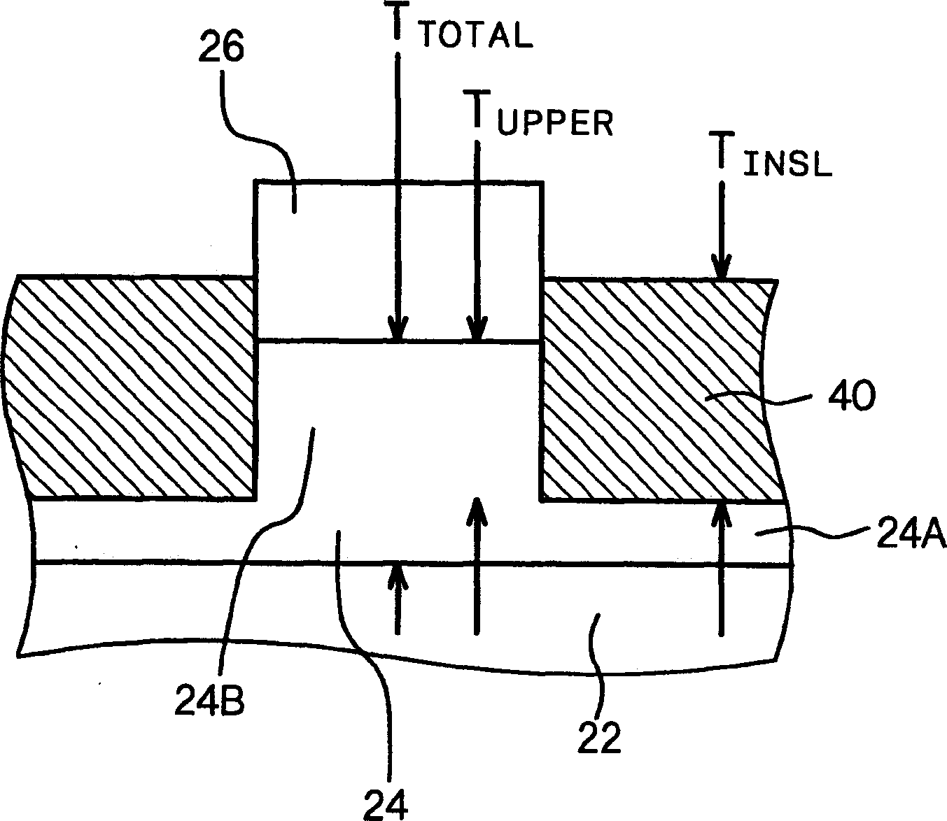
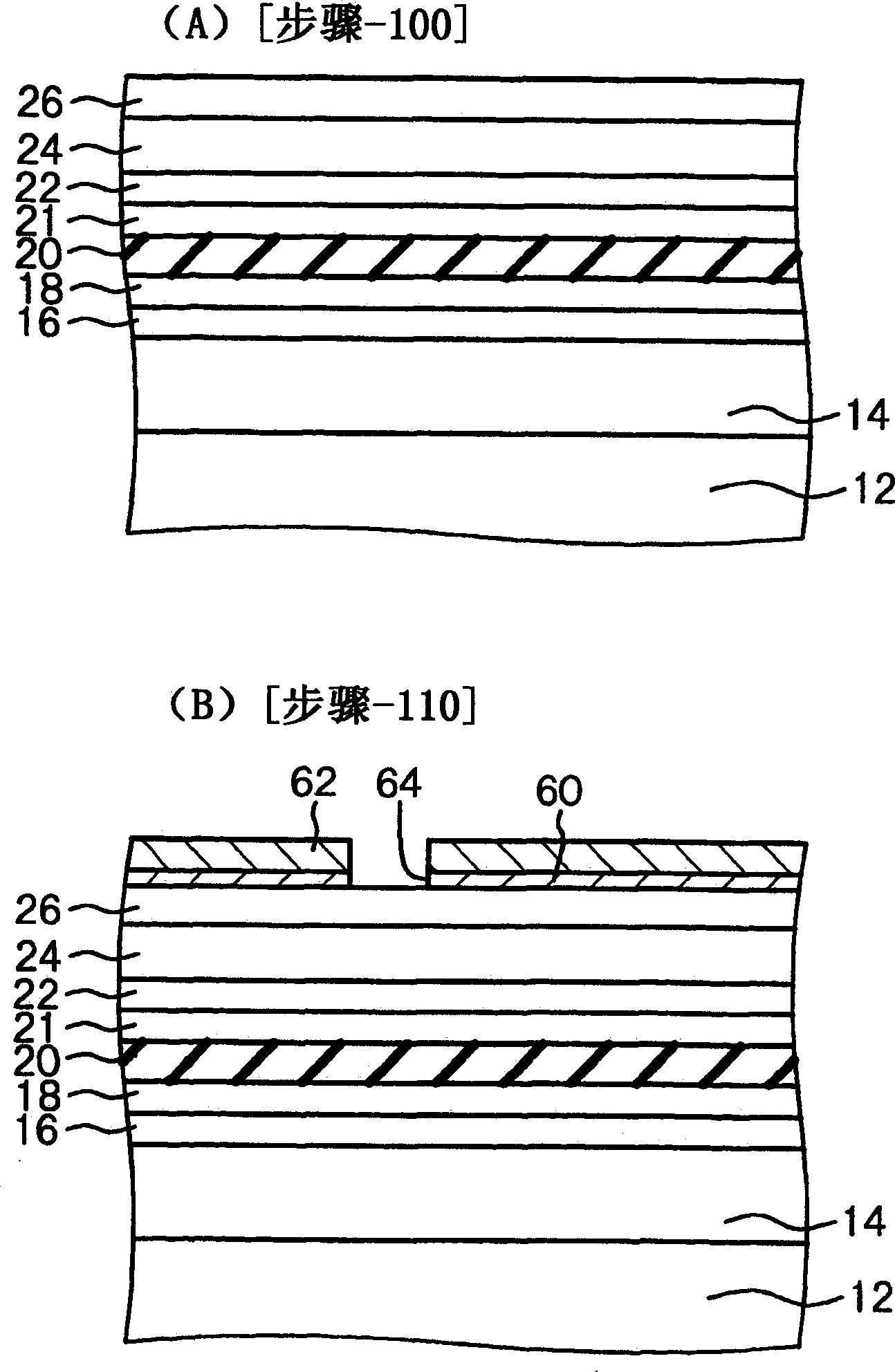
[0122] figure 1 is a schematic cross-sectional view of an index-guided nitrogen-based semiconductor laser device (refer to "semiconductor laser device 10" hereinafter) in Example 1. figure 2 is an enlarged schematic cross-sectional view of an element portion of the semiconductor laser device 10 . Among the reference numerals showing elements of the semiconductor laser device 10 in Example 1, the same reference numerals in FIG. 10 show the same elements in FIG. 10 .

[0123] As shown in the figure, the semiconductor laser device 10 in Example 1 includes:

[0124] (A) a first contact layer 14 made of n-type GaN and formed on a substrate 12 consisting of, for example, a sapphire substrate having a C-plane as a main surface,

[0125] (B) forming the first electrode 32 on the first contact layer 14,

[0126] (C) forming the first cladding layer 16 made of n-type AlGaN on the first contact layer 14,

[0127] (D) forming an active layer 20 on the first cladding layer 16, the act...


PUM


Abstract

The nitride-based semiconductor laser device 10 has a stacked structure comprising a first contacting layer 14, a first cladding layer 16, an active layer 20, a second cladding layer 24, a second contacting layer 26 and a second electrode 30 which are consecutively stacked, the second cladding layer 24 comprises a lower layer 24A and an upper layer 24B, the first cladding layer 14, the active layer 20 and the lower layer 24A of the second cladding layer have a mesa structure, the upper layer 24B of the second cladding layer and the second contacting layer 26 have a ridge structure, an insulating layer 40 covering at least part of each of both side surfaces of the upper layer 24B of the second cladding layer is formed on the portions of the lower layer 24A of the second cladding layer which portions correspond to the top surface of the mesa structure, and further, a metal layer 42 having substantially the same width as the mesa structure is formed on the top surface of the insulating layer 40 and the top surface of the second electrode 30 such that the metal layer 42 continues from one top surface to the other.

Description

Technical field: [0001] The present invention relates to a nitrogen-based semiconductor laser device and a production method thereof, more particularly, to a nitrogen-based semiconductor laser device having an operating voltage controllable at a desired value and having excellent transverse mode stability, and A nitrogen-based semiconductor laser for producing a nitrogen-based semiconductor laser having an operating voltage controllable at a desired value and having excellent transverse mode stability, wherein the production process is simplified. Background technique: [0002] A GaN-based semiconductor laser device with a GaN-based compound semiconductor layer stack structure formed on a sapphire substrate or a GaN substrate, as a light-emitting device, emits light in the short-wavelength region from the ultraviolet region to the green region, and is attracting Lots of attention. [0003] The composition of GaN-based semiconductor laser 100 disclosed in JP-A-2000-196201 wi...

Claims


Application Information

Patent Timeline
Patent Type & Authority Applications(China)
IPC IPC(8): H01S5/223H01L33/00H01S5/02H01S5/042H01S5/22H01S5/32H01S5/323H01S5/343
CPCH01S5/0425H01S2304/04H01S5/0422H01S5/2214H01S5/3072H01S5/22H01S5/32341B82Y20/00H01S5/2224H01S5/222H01S5/34333H01S5/0421H01S5/2231H01S5/0213H01S5/3213H01S2304/12H01S5/04257H01S5/04252H01S5/32
Inventor 山口恭司小林高志小林俊雅喜岛悟富冈聪安斋信一东条刚
Owner SONY CORP
Features
  • Generate Ideas
  • Intellectual Property
  • Life Sciences
  • Materials
  • Tech Scout
  • Unparalleled Data Quality
  • Higher Quality Content
  • 60% Fewer Hallucinations
Learn More