Semiconductor engineering recording equipment

A technology for recording equipment and semiconductors, applied in semiconductor/solid-state device manufacturing, electrical components, circuits, etc., can solve problems such as overheating burnout, radiation plate burnout, endpoint device component damage, etc., and achieve the effect of reducing production costs and speed.

Inactive Publication Date: 2003-12-03
MACRONIX INT CO LTD
View PDF0 Cites 0 Cited by
  • Summary
  • Abstract
  • Description
  • Claims
  • Application Information

AI Technical Summary

Problems solved by technology

Since the generated feedback signal SF usually has a high voltage pulse, the feedback signal SF often causes damage to the components in the endpoint device 10
For example, the radiation board in the endpoint device 10 will be burned due to the feedback signal SF, resulting in the entire endpoint device 10 being unusable
Especially for a process using a discrete plasma source (DPS), since the terminal device 10 must maintain a long-term output power, that is, the radio frequency module (not shown) must continue to operate, so the radiation board in the terminal device 10 Electronics on (Emission Board) (not shown) provide continuous load
As a result, the radiation board in the endpoint device 10 is more likely to be overheated and burned due to the feedback signal SF generated by the existing semiconductor process recording device 11
[0004] As a result, in the semiconductor manufacturing process using the existing semiconductor process recording equipment 11, it is necessary to replace the new terminal equipment 10 to restore the progress of the semiconductor process, resulting in an increase in production costs
Furthermore, the time it takes to frequently replace the endpoint device 10 can greatly reduce the throughput rate of semiconductor manufacturing

Method used


Image

  • Semiconductor engineering recording equipment
  • Semiconductor engineering recording equipment
  • Semiconductor engineering recording equipment

Examples


Embodiment Construction

[0028] The aforementioned and other objects, features, and advantages of the present invention will be more apparent with reference to the following detailed description and accompanying drawings. Preferred embodiments according to the present invention will be described in detail with reference to the drawings.

[0029] Example.

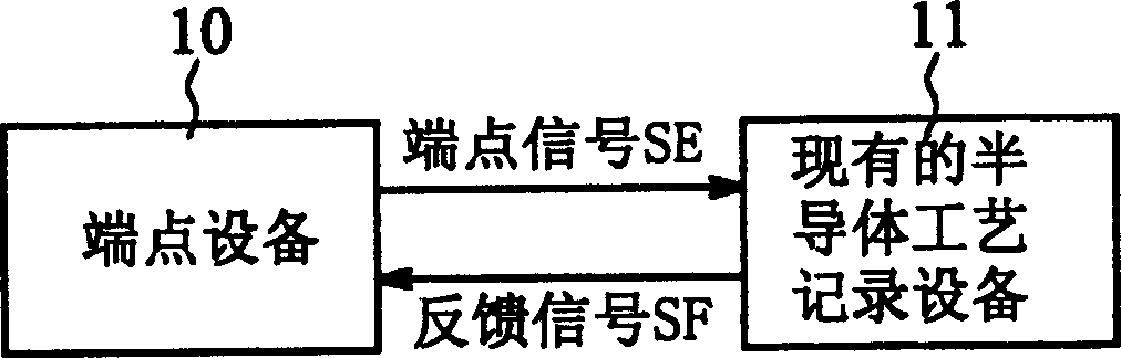
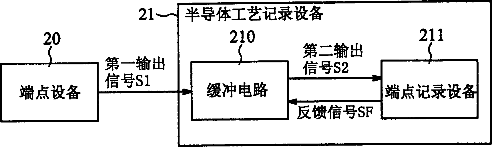
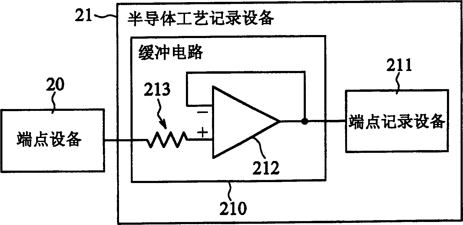
[0030] Figure 2A is a circuit block diagram showing a semiconductor process recording apparatus according to a first embodiment of the present invention. Such as Figure 2A As shown, the semiconductor process recording equipment 21 according to the first embodiment of the present invention includes a buffer circuit 210 and an endpoint recording device 211 . The endpoint recording device 211 according to the present invention may be as figure 1 Existing semiconductor process recording equipment 11 or the like is shown. The semiconductor process recording device 21 is connected to an external endpoint device 20 for recording the working status o...


PUM


Abstract

A semiconductor technology record device is composed of a buffer and a terminal recorder. The input of said buffer is connected to an external terminal equipment for receiving the first signal output from the external terminal equipment. The output of said buffer is connected to the terminal recorder for outputting the second signal as the response to the first one. When the terminal recorder receives said the second signal, a feedback signal is output to the buffer for isolating it by the buffer, so avoiding the damage of said feedback signal to the terminal equipment and greatly decreasing its cost.

Description

field of invention [0001] The invention relates to a semiconductor process recording device. More particularly, the present invention relates to a semiconductor process recording device that prevents burnout of terminal devices connected thereto. Background technique [0002] In the existing semiconductor manufacturing process, when the circuit system in the terminal machine outputs a signal to the existing semiconductor process recording equipment, the existing semiconductor process recording equipment will generate a feedback signal with a high voltage pulse to the terminal machine circuit system. The feedback signal often causes the components of the circuit system in the terminal machine, such as the emission board, to burn out, which increases the production cost of semiconductor manufacturing. The following will refer to figure 1 The problems posed by this existing semiconductor process recording equipment are described in detail. [0003] Such as figure 1 As show...

Claims


Application Information

Patent Timeline
Patent Type & Authority Applications(China)
IPC IPC(8): H01L21/00
Inventor 王宏翔游顺全刘邦开林育安陈委辰刘信成
Owner MACRONIX INT CO LTD
Why Eureka
Try Eureka