The invention discloses a process for making masking type read-only memory

A read-only memory and manufacturing method technology, which is applied in semiconductor/solid-state device manufacturing, electrical components, circuits, etc., can solve problems such as the increase of the resistance value of the buried bit line, and achieve the purpose of avoiding the short channel effect and the resistance value increase. Effect

Inactive Publication Date: 2003-12-31
MACRONIX INT CO LTD
View PDF0 Cites 0 Cited by
  • Summary
  • Abstract
  • Description
  • Claims
  • Application Information

AI Technical Summary

Problems solved by technology

However, although the source / drain regions of shallow junctions or ultra-shallow junctions can improve the problem of short channel effects caused by device shrinkage, but due to the shallow depth / junction of buried bit lines, it will lead to buried The resistance of the in-line bit line increases

Method used


Image

  • The invention discloses a process for making masking type read-only memory
  • The invention discloses a process for making masking type read-only memory
  • The invention discloses a process for making masking type read-only memory

Examples


Embodiment Construction

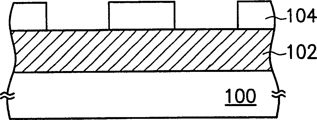
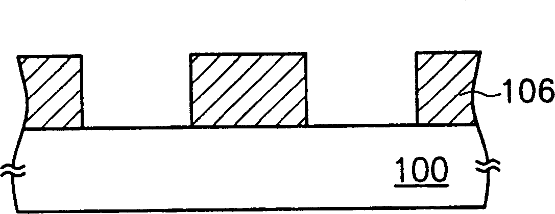
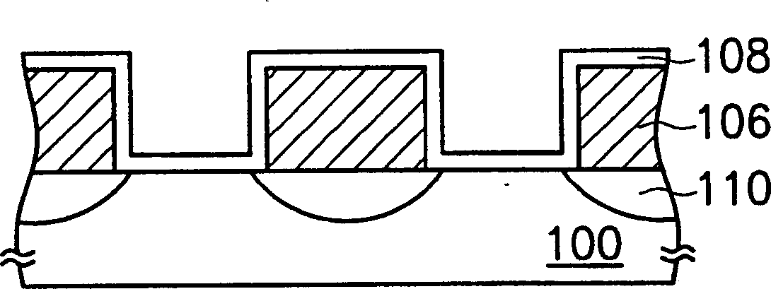
[0024] The invention provides a method for manufacturing a mask type read-only memory. Figure 1A to Figure 1D Shown is a cross-sectional view of the manufacturing process of a mask-type ROM according to a preferred embodiment of the present invention.

[0025] First, please refer to Figure 1A , providing a substrate 100, such as a semiconductor silicon substrate. Next, a doped conductor layer 102 is formed on the substrate 100 . The material of the doped conductive layer 102 is, for example, polysilicon doped with ions. The method of forming the doped conductive layer 102 is, for example, to form a layer of doped polysilicon on the substrate 100 by doping ions on site by chemical vapor deposition. layer. The doped ions are, for example, phosphorus ions, and the doped dose is, for example, 0.5*10 19 to 0.5*10 21 1 / cm 3 about. Doped ions can also use arsenic ions, and the doped dose is, for example, 0.5*10 19 to 0.5*10 21 1 / cm 3 about. Then, a patterned mask layer 10...


PUM


Abstract

The invention discloses a process for making masking type read-only memory wherein a substrate is provided, and a doping conductor layer is formed on the substrate. Then a plurality of bar shape doping conductor layers are formed by figuring the doping conductor layer, and a dielectric layer is formed on the substrate and the bar shape doping conductor layer, at the same time, a plurality of diffusion zones are formed on the substrate under the bar shape doping conductor layer. Later, the figured conductor layer is formed on the dielectric layer.

Description

technical field [0001] The present invention relates to a method for manufacturing a read-only memory (Read Only Memory, ROM), and in particular to a method for manufacturing a mask-type read-only memory (Mask ROM). Background technique [0002] Since the read-only memory has the non-volatile characteristic that the data stored therein will not be lost due to power interruption, many electrical products must have this type of memory to maintain the normal operation of the electrical product when it is turned on. The most basic type of read-only memory is masked read-only memory. The commonly used masked read-only memory uses channel transistors as memory cells, and selectively implants ions into In the specified channel area, the purpose of controlling the memory cell to be turned on (On) or turned off (Off) during the read operation is achieved by changing the threshold voltage (Threshold Voltage). [0003] The structure of a general masked read-only memory is that the pol...

Claims


Application Information

Patent Timeline
Patent Type & Authority Applications(China)
IPC IPC(8): H01L21/8246
Inventor 范左鸿叶彦宏詹光阳刘慕义
Owner MACRONIX INT CO LTD
Why Eureka
Try Eureka