Integration of phosphorus emitter in an NPN device in a BiCMOS process

a technology of phosphorus emitter and bicmos process, which is applied in the direction of semiconductor devices, electrical apparatus, transistors, etc., can solve the problems of reducing the performance of npn devices, reducing the activation of arsenic, and becoming more difficult to transparently integrate high-performance bipolar devices, etc., and achieves low emitter resistance.

Active Publication Date: 2009-03-03
NEWPORT FAB
View PDF6 Cites 2 Cited by
  • Summary
  • Abstract
  • Description
  • Claims
  • Application Information

AI Technical Summary

Benefits of technology

[0009]The present invention is directed to method and structure for integrating a phosphorus emitter in an NPN device in a BiCMOS process. The present invention overcomes the need in the art for an NPN device having a low emitter resistance and a shallow emitter-base junction that can be effectively integrated with a CMOS device in a BiCMOS process.

Problems solved by technology

As Bipolar Complementary-Metal-Oxide-Semiconductor (“BiCMOS”) technology continues to advance in an effort to achieve increased device speed and reduced power consumption, it becomes more difficult to transparently integrate high performance bipolar devices, such as high performance NPN devices, with CMOS devices.
However, the reduced thermal budget results in lower activation of arsenic and, consequently, increased emitter resistance, which reduces NPN device performance.
However, the high diffusion coefficient of phosphorus causes phosphorus to diffuse significantly into the base region of the NPN device during RTP.
As a result, phosphorus causes an undesirably deep emitter-base junction to be formed in the NPN device, which reduces performance of the NPN device.

Method used


Image

  • Integration of phosphorus emitter in an NPN device in a BiCMOS process
  • Integration of phosphorus emitter in an NPN device in a BiCMOS process
  • Integration of phosphorus emitter in an NPN device in a BiCMOS process

Examples


Embodiment Construction

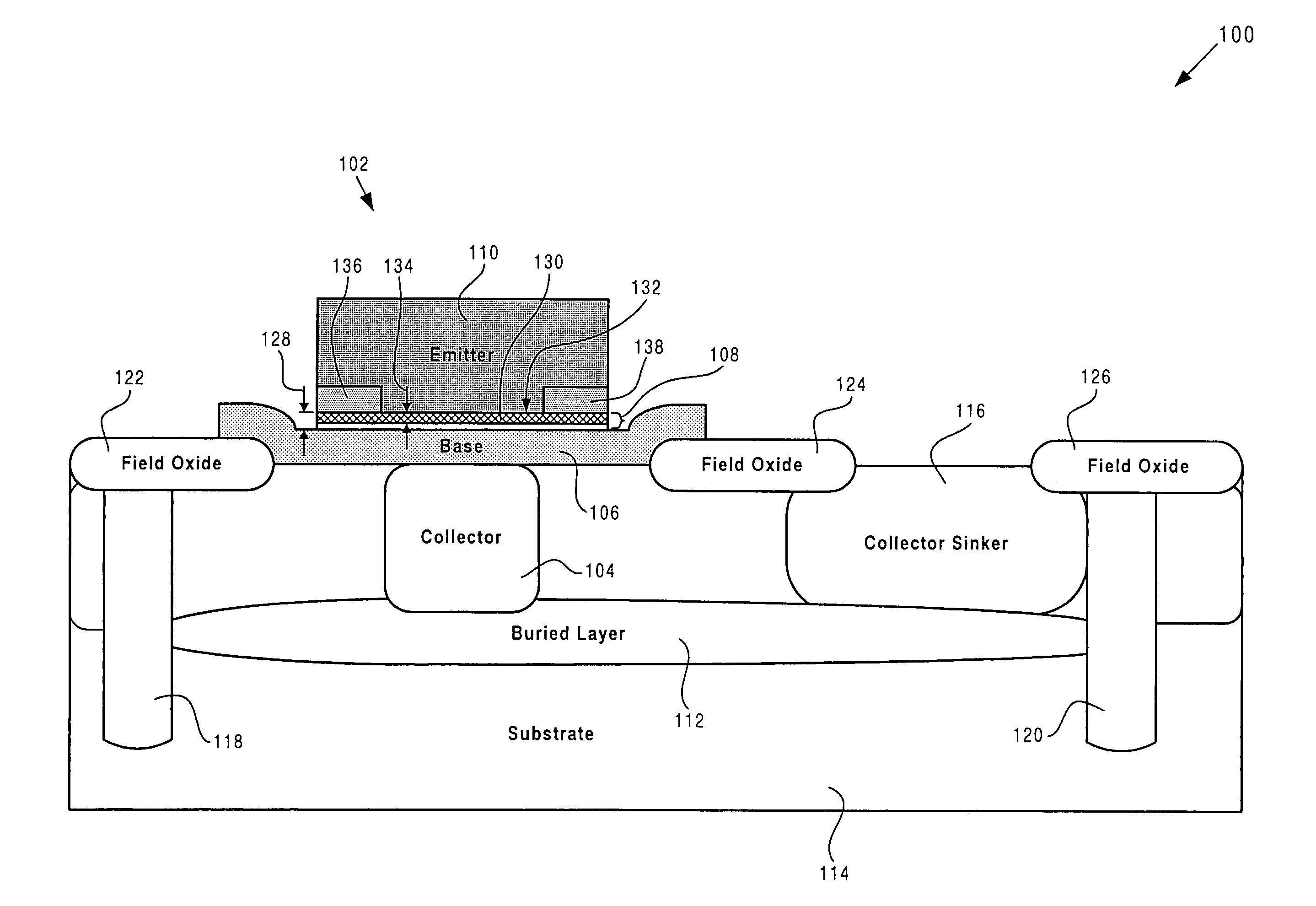
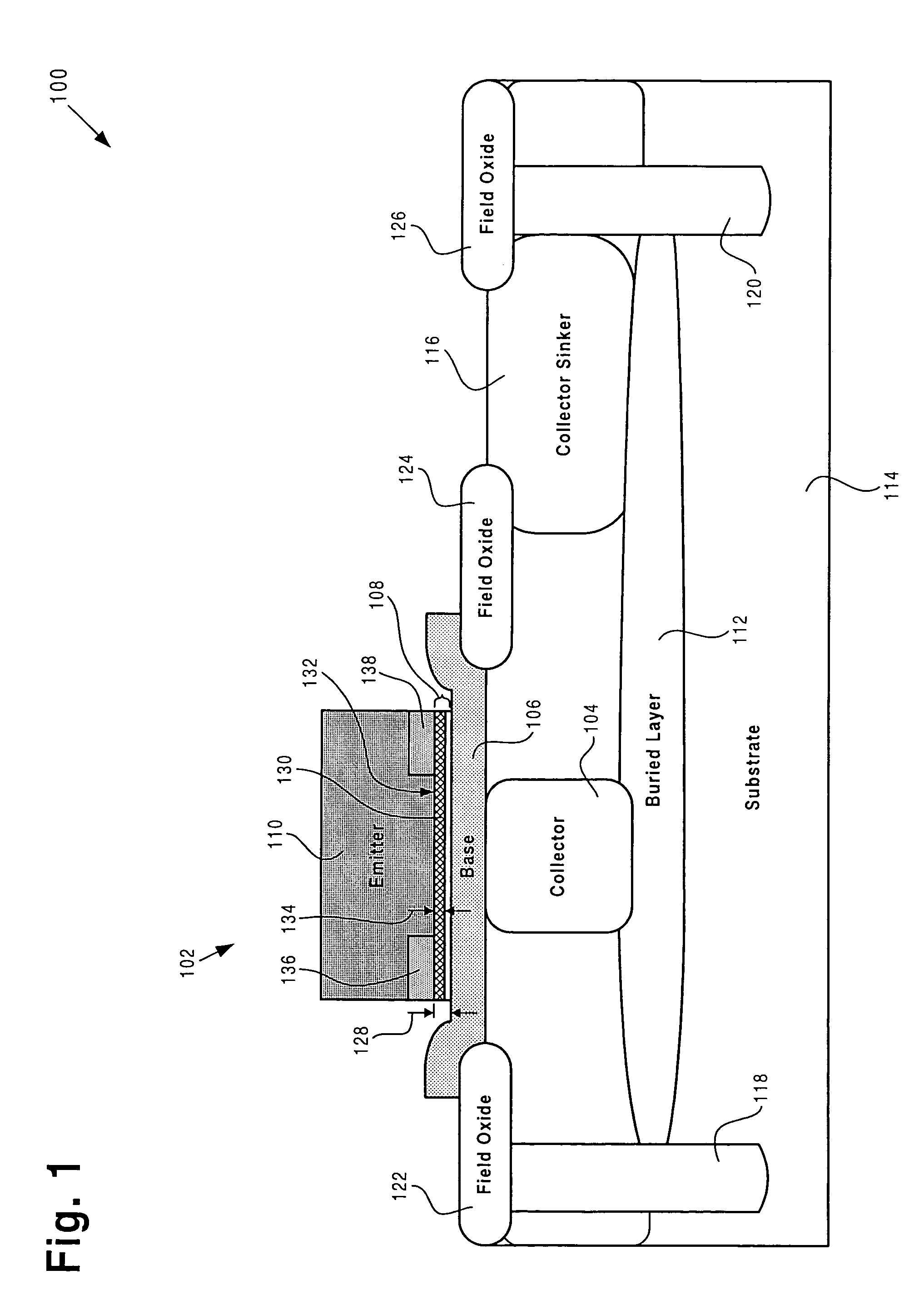
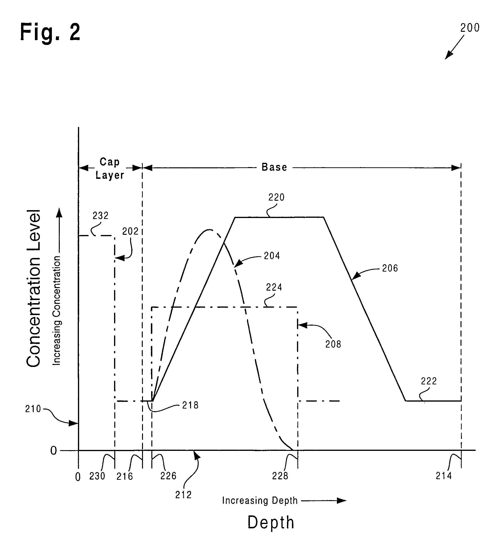
[0015]The present invention is directed to method and structure for integrating a phosphorus emitter in an NPN device in a BiCMOS process. The following description contains specific information pertaining to the implementation of the present invention. One skilled in the art will recognize that the present invention may be implemented in a manner different from that specifically discussed in the present application. Moreover, some of the specific details of the invention are not discussed in order not to obscure the invention. The specific details not described in the present application are within the knowledge of a person of ordinary skill in the art.

[0016]The drawings in the present application and their accompanying detailed description are directed to merely exemplary embodiments of the invention. To maintain brevity, other embodiments of the invention which use the principles of the present invention are not specifically described in the present application and are not specif...


PUM


Abstract

According to one exemplary embodiment, a heterojunction bipolar transistor includes a base situated on a substrate. The heterojunction bipolar transistor can be an NPN silicon-germanium heterojunction bipolar transistor, for example. The heterojunction bipolar transistor further includes a cap layer situated on the base, where the cap layer includes a barrier region. The barrier region can comprises carbon and has a thickness, where the thickness of the barrier region determines a depth of an emitter-junction of the heterojunction bipolar transistor. An increase in the thickness of the barrier region can cause a decrease in the depth of the emitter-base junction. According to this exemplary embodiment, the heterojunction bipolar transistor further includes an emitter situated over the cap layer, where the emitter comprises an emitter dopant, which can be phosphorus. A diffusion retardant in the barrier region of the cap layer impedes diffusion of the emitter dopant.

Description

[0001]This is a continuation of application Ser. No. 10 / 997,534 filed Nov. 23, 2004 now U.S. Pat. No. 7,297,992.BACKGROUND OF THE INVENTION[0002]1. Field of the Invention[0003]The present invention is generally in the field of fabrication of semiconductor devices. More specifically, the invention is in the field of fabrication of bipolar transistors.[0004]2. Related Art[0005]As Bipolar Complementary-Metal-Oxide-Semiconductor (“BiCMOS”) technology continues to advance in an effort to achieve increased device speed and reduced power consumption, it becomes more difficult to transparently integrate high performance bipolar devices, such as high performance NPN devices, with CMOS devices. High performance NPN devices, such as NPN silicon-germanium (SiGe) heterojunction bipolar transistors (HBT), require a shallow emitter-base junction and low emitter resistance while CMOS devices require a CMOS process with a low thermal budget for advanced BiCMOS technology.[0006]By way of background, ...

Claims


Application Information

Patent Timeline
Patent Type & Authority Patents(United States)
IPC IPC(8): H01L29/739
CPCH01L21/8249H01L27/0623H01L29/7378H01L29/0821H01L29/66242H01L29/0817
Inventor U'REN, GREG D.
Owner NEWPORT FAB
Why Eureka
Try Eureka