Fabrication method of semiconductor device

a technology of semiconductor devices and fabrication methods, which is applied in the direction of semiconductor devices, electrical equipment, transistors, etc., can solve the problems of difficult to increase the depth of a source/drain of a microfabricated transistor, no improvement in the junction leakage current, and no effect in the nickel silicide formation process, so as to reduce the thickness of the nickel silicide film, suppress the junction leakage current, and speed up the diffusion speed of metal diffusion in the source/drain region.

Active Publication Date: 2010-12-14
PANNOVA SEMIC
View PDF15 Cites 0 Cited by
  • Summary
  • Abstract
  • Description
  • Claims
  • Application Information

AI Technical Summary

Benefits of technology

[0013]Another solution for the above problem may be to form the P type source / drain region deeper than the depth of the abnormally-grown nickel silicide. However, as mentioned earlier, it is difficult to increase the depth of a source / drain of a microfabricated transistor because of the need to reduce the depth of an impurity diffusion layer, which constitutes the source / drain and the like, to suppress short-channel effects.
[0014]The present invention was made to solve the above problem. An object of the present invention is to provide a fabrication method of a semiconductor device in which abnormal growth of silicide during formation of the silicide is suppressed in a P channel type MOS transistor, thereby suppressing increase injunction leakage current flowing from a source / drain region to a well, while maintaining shallow junction of the source / drain region.
[0016]According to this method, a silicon crystal is once made amorphous by implanting the first element, which is larger than silicon, during formation of the source / drain regions and then recrystallized by a subsequent heat treatment. Crystal defects remaining in the source / drain regions can be corrected by this process. Moreover, speed of diffusion at which the metal diffuses in the source / drain regions can be slowed down because a large amount of elements larger than silicon exists in the source / drain regions. As a result, it is possible to reduce a thickness of the nickel silicide film and suppress junction leakage current.

Problems solved by technology

However, when argon is selected as an element whose atomic radius is greater than that of silicon and which does not cause chemical reaction with silicon and does not generate a level in the silicon for forming nickel silicide by the above method, no improvement was found in the junction leakage current flowing from the P type source / drain region to the well in the P channel type transistor, and no effect was found in the nickel silicide formation process.
However, as mentioned earlier, it is difficult to increase the depth of a source / drain of a microfabricated transistor because of the need to reduce the depth of an impurity diffusion layer, which constitutes the source / drain and the like, to suppress short-channel effects.

Method used


Image

  • Fabrication method of semiconductor device
  • Fabrication method of semiconductor device
  • Fabrication method of semiconductor device

Examples


embodiment

[0023]An example of a semiconductor device fabrication method of the present invention is hereinafter described, with reference to the drawings. Although a P channel type MIS transistor and an N channel type MIS transistor are formed alternately in the transistor fabrication process, descriptions of a fabrication process of an N channel type MIS transistor is omitted here because the present invention relates to a fabrication method of a P channel type MIS transistor.

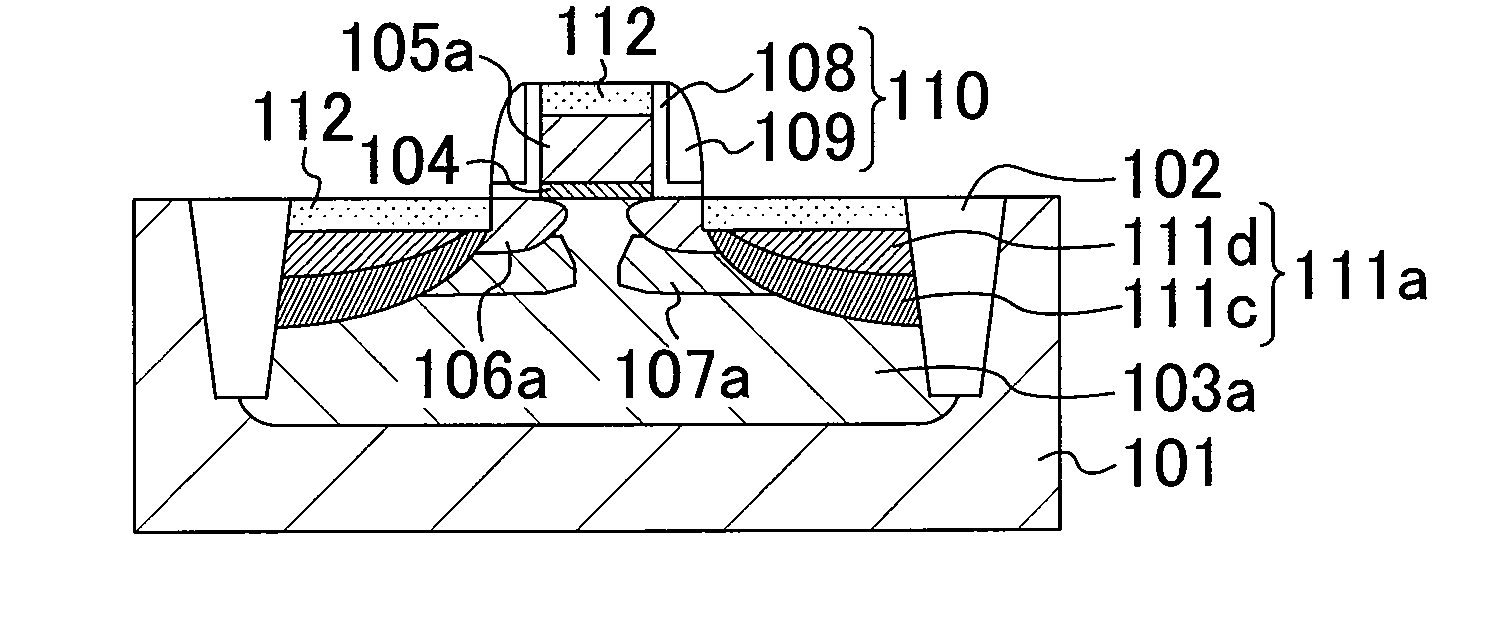
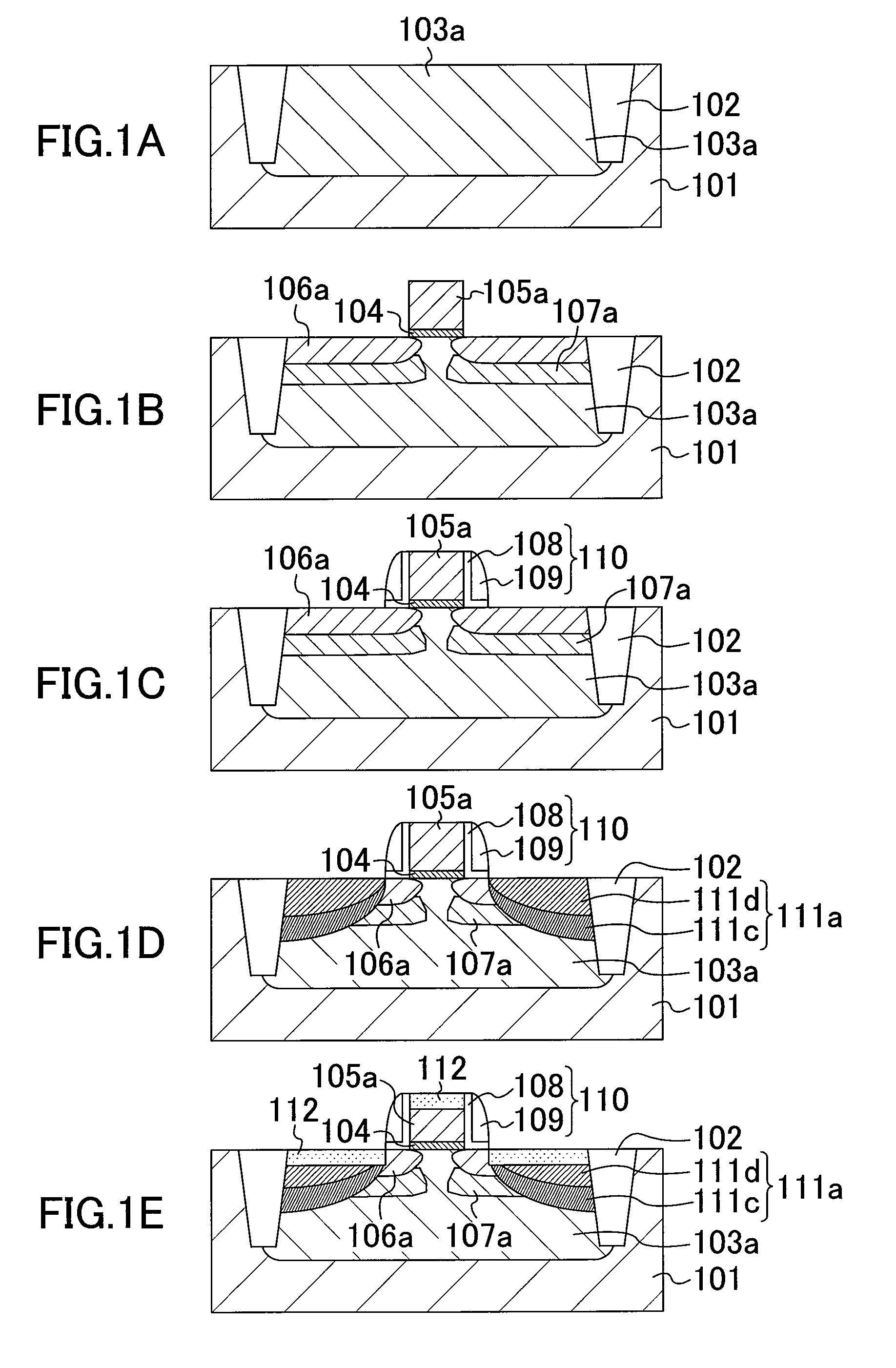
[0024]FIG. 1A to FIG. 1E are cross sections showing a fabrication method of a semiconductor device according to the first embodiment of the present invention. This semiconductor device includes a P channel type MOS transistor on an N type well 103a.

[0025]First, as shown in FIG. 1A, an isolation region 102 composed of a buried insulating film or the like is formed in a semiconductor substrate 101 of silicon or the like. After that, the N type well 103a is formed by photolithography and ion implantation.

[0026]Then, as sh...


PUM


Abstract

A fabrication method of a semiconductor device includes: forming a gate insulating film and a gate electrode on an N type well; forming first source / drain regions by implanting a first element in regions of the N type well on both sides of the gate electrode, the first element being larger than silicon and exhibiting P type conductivity; forming second source / drain regions by implanting a second element in the regions of the N type well on the both sides of the gate electrode, the second element being smaller than silicon and exhibiting P type conductivity; and forming a metal silicide layer on the source / drain regions.

Description

CROSS-REFERENCE TO RELATED APPLICATION[0001]This application claims priority from Japanese Patent Application JP2008-018856 filed on Jan. 30, 2008, the disclosure of which application is hereby incorporated by reference into this application in its entirety for all purposes.BACKGROUND OF THE INVENTION[0002]A technology disclosed in this specification relates to a fabrication method of a semiconductor device, specifically to a method of forming a source / drain of a microfabricated P channel type MIS transistor in which nickel silicide is used.[0003]In recent years, the structure in which impurity diffusion layers constituting source / drain regions are formed as thinly as possible has been adopted to suppress short-channel effects associated with the microfabrication of transistors. However, the reduction in depth of the impurity diffusion layers results in increase in sheet resistance of the impurity diffusion layers. As a result, it becomes difficult to achieve high-speed operation an...

Claims


Application Information

Patent Timeline
Patent Type & Authority Patents(United States)
IPC IPC(8): H01L21/02
CPCH01L29/1083H01L29/665H01L29/6659H01L29/7833
Inventor KAMADA, HIROYUKI
Owner PANNOVA SEMIC
Why Eureka
Try Eureka