Semiconductor device and a method of manufacturing a semiconductor device

a semiconductor and semiconductor technology, applied in the direction of semiconductor devices, radiation controlled devices, electrical devices, etc., can solve the problems of low reliability of light receiving elements in which the gate oxide film 104/b> has a deteriorated quality, the quality of the insulating film may be deteriorated, and the manufacturing process may be affected

Active Publication Date: 2018-08-07
ABLIC INC
View PDF3 Cites 0 Cited by
  • Summary
  • Abstract
  • Description
  • Claims
  • Application Information

AI Technical Summary

Benefits of technology

[0021]According to the embodiment of the present invention, the second thermal oxide film is newly formed after the first thermal oxide film other than that under the gate electrode is removed. Thus, the thermal oxide film, which is not damaged through etching in the patterning of the polysilicon film, can be an insulating film that is in direct contact with the surface of the silicon substrate in the light receiving element forming region. Further, the thickness of the second thermal oxide film can be set regardless of the thickness of the gate oxide film. Accordingly, by forming the second thermal oxide film, which has comparatively few charge traps, to have an appropriate thickness (for example, a thickness of 30 nm or less) and by performing ion implantation on the light receiving element forming region through the second thermal oxide film to form the impurity region, a dose amount in the ion implantation can be kept low, and there can be formed the light receiving element, which has a shallow junction in which an impurity concentration in the outermost surface of the silicon substrate in the impurity region is 1019 cm−3 or more, and a depth from the surface of the silicon substrate at which the impurity concentration in the impurity region becomes 1017 cm−3 or less is 100 nm or less.

Problems solved by technology

Hence, although the insulating film is a thermal oxide film, a quality of the insulating film may be deteriorated due to etching damage at the time of gate patterning.
Thus, the light receiving element in which the gate oxide film 104 having a deteriorated quality is in direct contact with the silicon surface has low reliability.
When ion implantation with this dose amount is performed at one time, failures, such as burning and sticking of a resist, may occur in the manufacturing process.
Further, since a junction depth becomes about 200 nm, a shallow junction of 100 nm or less, which is essentially needed to detect the ultraviolet light with high sensitivity, is not obtained.

Method used


Image

  • Semiconductor device and a method of manufacturing a semiconductor device
  • Semiconductor device and a method of manufacturing a semiconductor device
  • Semiconductor device and a method of manufacturing a semiconductor device

Examples


first embodiment

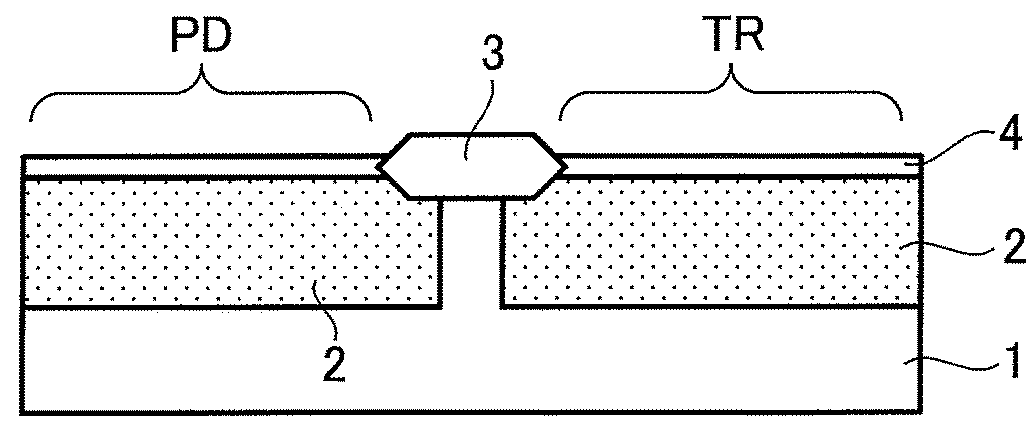
[0031]FIGS. 1A to 1E and FIGS. 2A to 2D are cross-sectional views for illustrating a method of manufacturing a semiconductor device of a first embodiment of the present invention in the order of steps.

[0032]In FIGS. 1A to 1E and FIGS. 2A to 2D, PD represents a light receiving element forming region in which a light receiving element is formed, and TR represents a MOS transistor forming region in which a PMOS transistor is formed.

[0033]First, as illustrated in FIG. 1A, N-well regions 2 and an element isolation region 3 are formed on a surface of a p-type silicon substrate 1, and then ion implantation for adjusting a threshold voltage of a transistor is performed as necessary.

[0034]Then, the entire surface of the silicon substrate 1 is thermally oxidized, to thereby form a gate oxide film (also referred to as “first thermal oxide film”) 4. The gate oxide film 4 has a thickness of 10 nm, for example.

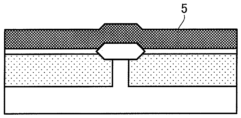
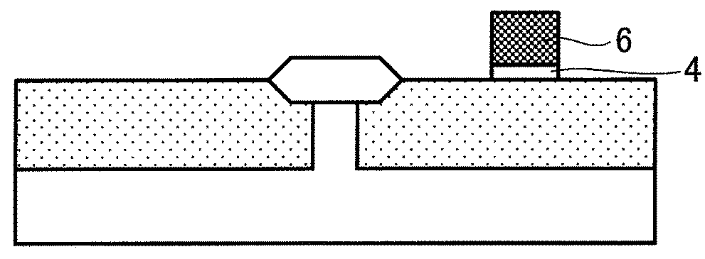
[0035]Next, a polysilicon film 5, which is a material of a gate electrode 6, is deposit...

second embodiment

[0045]FIGS. 3A and 3B are cross-sectional views for illustrating a manufacturing method of a second embodiment of the present invention in the order of steps. In FIG. 3A, the same step as that of FIG. 1D is illustrated. Steps up to this step are the same as those in the first embodiment, and the descriptions thereof are thus omitted. However, in this embodiment, the thickness of the thermal oxide film 7 is set to be 30 nm, which is thicker than that of the first embodiment.

[0046]In this state, as illustrated in FIG. 3B, ion implantation for forming a shallow junction is performed on the light receiving element forming region PD. The ion implantation conditions are BF2, 15 keV, and 5.3×1014 cm−2, for example. This ion implantation is also performed on the MOS transistor forming region TR, to thereby form the LDD regions 9.

[0047]After the step of FIG. 3B, the PMOS transistor and the light receiving element may be formed on the same silicon surface by following the same steps as illust...

third embodiment

[0052]FIGS. 4A to 4D are cross-sectional views for illustrating a manufacturing method of a third embodiment of the present invention in the order of steps. In FIG. 4A, the same step as that of FIG. 2A is illustrated. Steps up to this step are the same as those in the first embodiment, and the descriptions thereof are thus omitted.

[0053]Next, as illustrated in FIG. 4B, insulating films 10a and 10b for forming side walls are deposited. In this case, the insulating film 10a is a silicon nitride film having a thickness of 20 nm, and the insulating film 10b is a silicon dioxide film having a thickness of 280 nm. Further, the thermal oxide film 7 on the surface of the light receiving element forming region has a thickness of 30 nm or less.

[0054]Subsequently, as illustrated in FIG. 4C, side walls 11b including the insulating film (silicon dioxide film) 10b are formed on the side surfaces of the gate electrode 6 through anisotropic etching. Through use of etching conditions in which an etc...


PUM


Abstract

In order to form a light receiving element having high reliability and a MOS transistor together on the same silicon substrate, after forming a gate electrode of the MOS transistor, a gate oxide film in a light receiving element forming region is removed. Then, a thermal oxide film is newly formed in the light receiving element forming region, and ion implantation is performed in the light receiving element forming region through the thermal oxide film such that a shallow pn junction is formed.

Description

BACKGROUND OF THE INVENTION[0001]1. Field of the Invention[0002]The present invention relates to a semiconductor device and a method of manufacturing a semiconductor device, and particularly, to a semiconductor device and a method of manufacturing a semiconductor device, in which a semiconductor light receiving element configured to detect short-wavelength light, for example, an ultraviolet light, and a MOS transistor are formed on the same silicon substrate.[0003]2. Description of the Related Art[0004]There are various types of semiconductor light receiving elements. Among those semiconductor light receiving elements, a light receiving element formed on a silicon substrate is used in many applications. This is because, by forming an integrated circuit including a MOS transistor or the like and the light receiving element on the same substrate, a process from receiving light to processing a signal can be conducted on one chip.[0005]A penetration depth of light in silicon (a depth at...

Claims


Application Information

Patent Timeline
Patent Type & Authority Patents(United States)
IPC IPC(8): H01L27/146H01L29/66H01L29/78
CPCH01L27/14689H01L27/14616H01L27/14685H01L29/7833H01L29/66492H01L21/265H01L29/66477H01L29/78H01L31/101H01L31/18H01L29/6659H01L27/1461H01L27/14614
Inventor FUTATSUGI, TOSHIRO
Owner ABLIC INC
Why Eureka
Try Eureka