Method for reducing cracking and deformation of copper wire

A copper layer and semiconductor technology, applied in the direction of semiconductor devices, semiconductor/solid-state device manufacturing, electrical components, etc., can solve the problems of cracks, abnormal opening resistance, stress imbalance, etc., and achieve the effect of cost economy

Inactive Publication Date: 2004-02-11
UNITED MICROELECTRONICS CORP
View PDF0 Cites 13 Cited by
  • Summary
  • Abstract
  • Description
  • Claims
  • Application Information

AI Technical Summary

Problems solved by technology

Since this deposition process is a part of the inevitable heat treatment in the subsequent process, the temperature is very high. Therefore, for the double-layer embedded copper particles under the dielectric layer 204A, the stress imbalance will be caused by this heat treatment ( stress imbalance), resulting in cracks or abnormal openings and excessive resistance

Method used


Image

  • Method for reducing cracking and deformation of copper wire
  • Method for reducing cracking and deformation of copper wire
  • Method for reducing cracking and deformation of copper wire

Examples


Embodiment Construction

[0031] Preferred embodiments of the present invention will be discussed in detail as follows. The embodiment is used to describe a specific example of using the present invention, but not to limit the scope of the present invention.

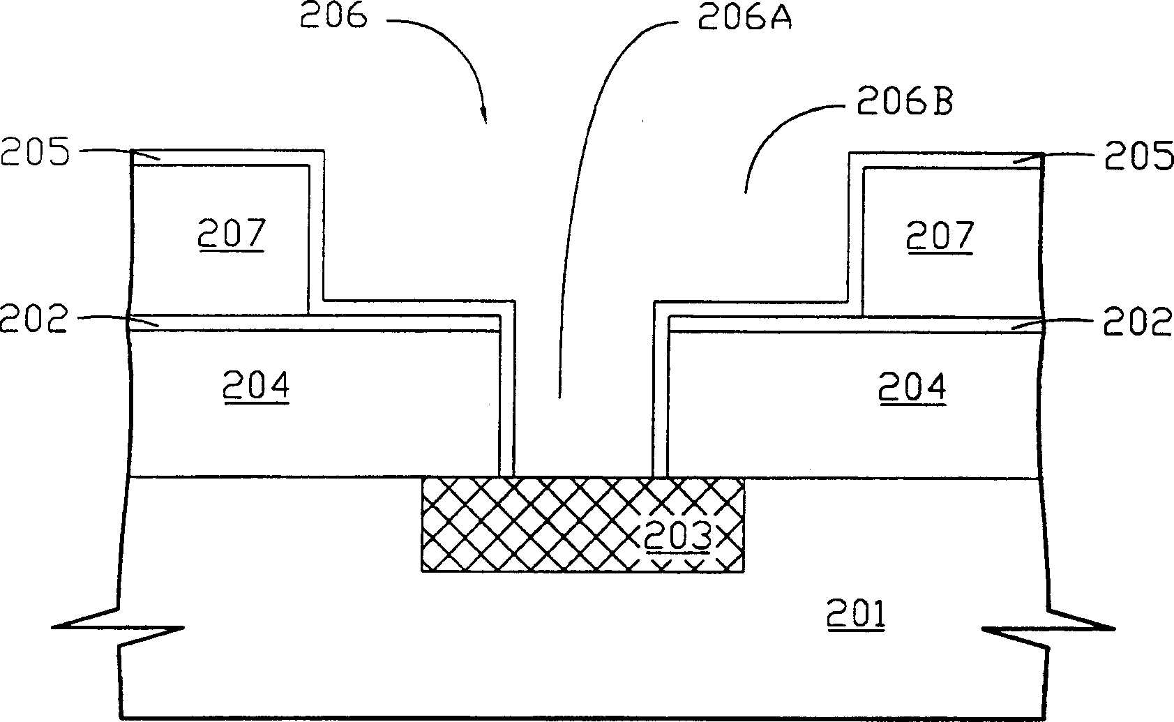
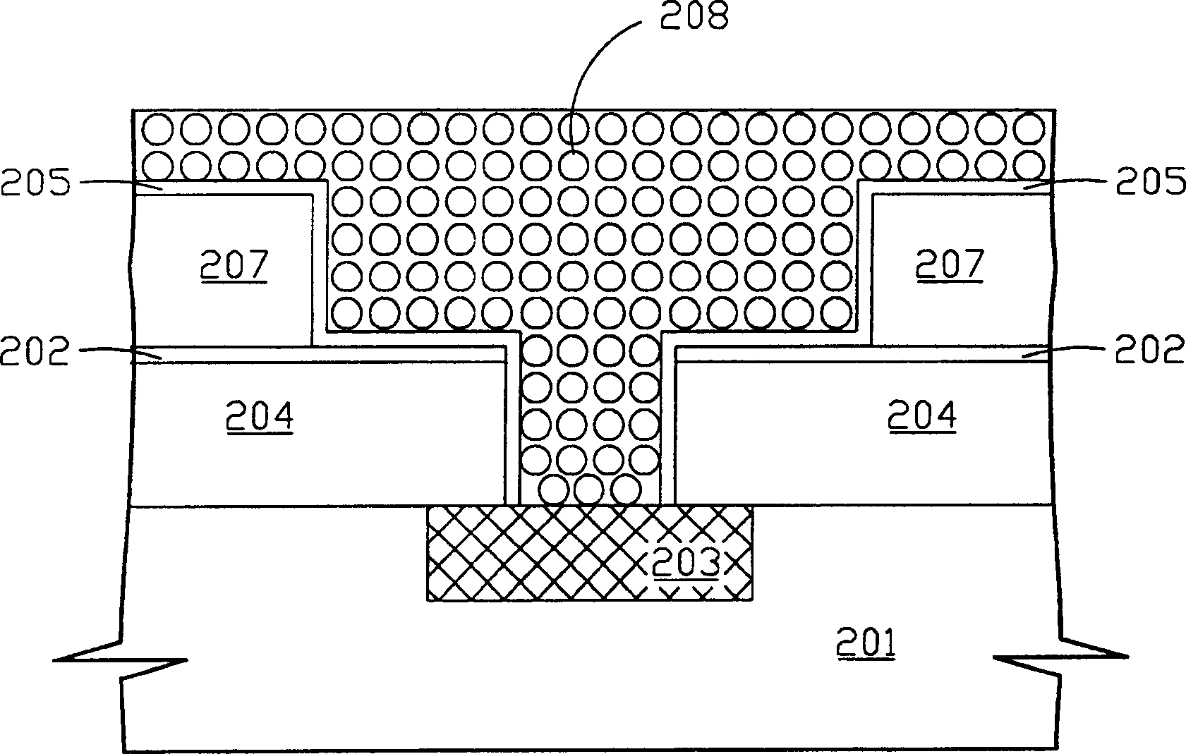
[0032] In addition, various parts of the semiconductor device are not drawn to scale. Certain dimensions have been exaggerated compared to other relevant dimensions to provide a clearer description and understanding of the invention.

[0033] Although the embodiments shown here are shown in two dimensions with widths and depths in different stages, it should be clearly understood that the regions shown are only part of a three-dimensional cell of a wafer where the wafer may Contains many unit cells arranged in three dimensions. In contrast, in the manufacture of actual components, illustrated regions have three-dimensional length, width and height.

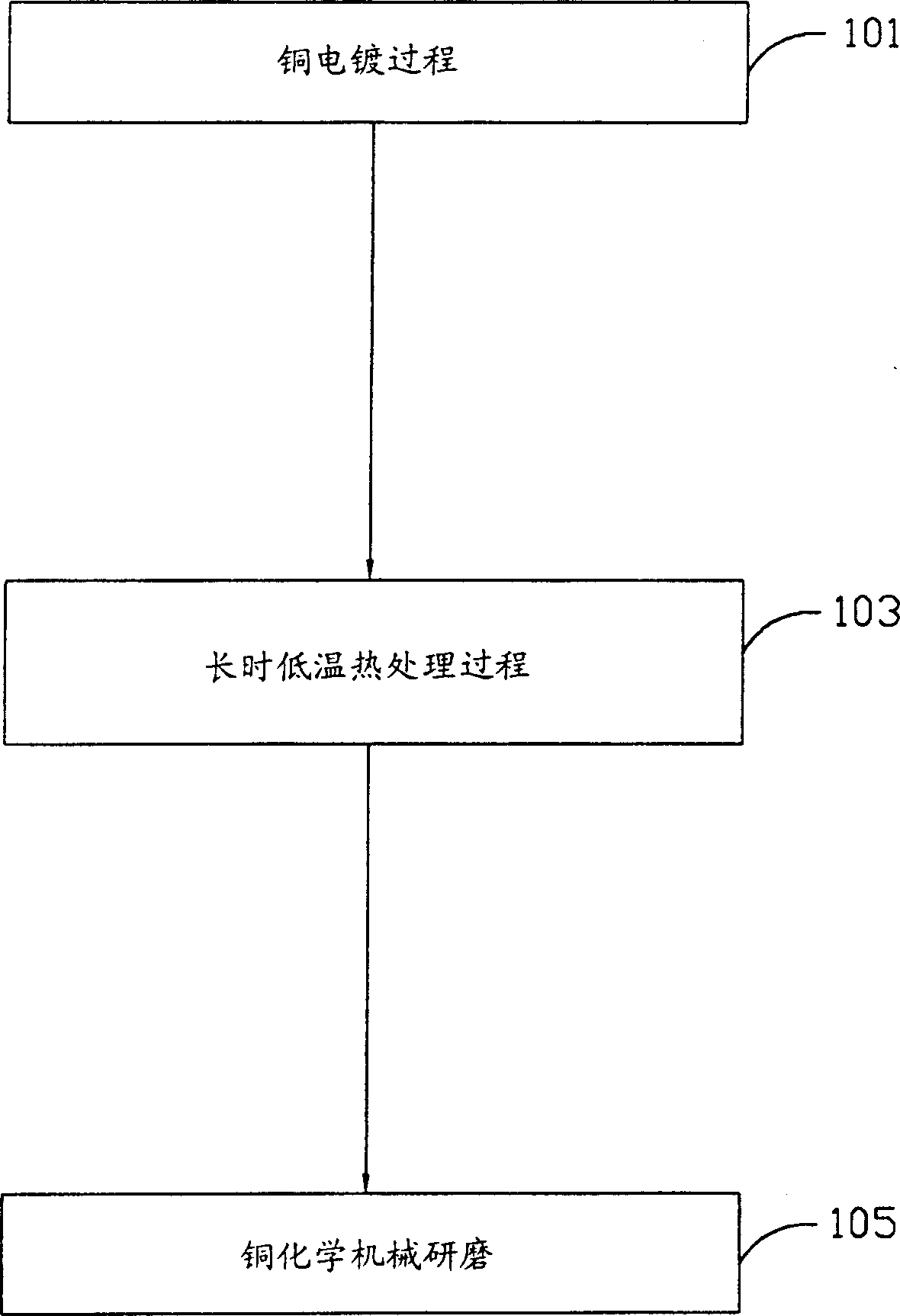
[0034] Figure 4, represents the flow chart of forming the copper interconnection in the pres...


PUM


Abstract

A method for reducing copper wire cracking and deformation includes exerting a short term high-temp. heat treatment, during a long term low-temp. heat treatment to strengthen the internal stress of copper. The high-temp. means which is the highest temp. from the beginning of long term low-temp. heat treatment to the end of interconnection line metallization process, namely working temp. Under thesaid high-temp. rapid heating to strength copper film stress and maturate the copper grains. Therefore, in the followed process, temperature is below the highest temperature, the copper film structure becomes more stable and cracking can be reduced to a lowest degree.

Description

(1) Technical field [0001] The invention relates to a method for forming copper wires in a semiconductor element manufacturing process, in particular to a method for reducing cracks and deformation of copper wires by means of short-term high temperature in a thermal process. (2) Background technology [0002] In the past VLSI process technology, a typical metal oxide semiconductor structure is mainly composed of the following important process steps: [0003] 1. Form a field isolation zone; [0004] 2. Forming a conductive gate on the dielectric layer; [0005] 3. Heavily doped source and drain regions; [0006] 4. Depositing one or more dielectric layers to form an inner dielectric layer; [0007] 5. A contact opening is formed between the inner dielectric layers, and the source, drain and gate are electrically connected through the metal in the middle; [0008] 6. Depositing one or more metal layers for the metallization process; and [0009] 7. Form a protective film...

Claims


Application Information

Patent Timeline
Patent Type & Authority Applications(China)
IPC IPC(8): H01L21/768
CPCH01L21/76877
Inventor 刘正美江怡颖杨名声
Owner UNITED MICROELECTRONICS CORP
Why Eureka
Try Eureka