Key position arrangement method of film circuit board

A thin-film circuit board and button technology, which is applied in the direction of electrical digital data processing, input/output process of data processing, instruments, etc., can solve problems such as uneven thickness of thin-film circuits, increased production costs, and circuit isolation.

Inactive Publication Date: 2004-02-25
ZIPPY TECH
View PDF0 Cites 0 Cited by
  • Summary
  • Abstract
  • Description
  • Claims
  • Application Information

AI Technical Summary

Problems solved by technology

[0004] When making this kind of thin film circuit board with jumpers, not only are there many printing processes and complicated manufacturing steps, but the production cost is increased, the relative output is reduced, and the rate of defective products is also high. The proportion of short circuit is high, the reliability of the product is poor, and the jumper printing of the film circuit board is easy to cause the thickness of the film circuit to be uneven and affect the key in.
[0005] In addition, when the keyboard made by the above method is operated by the user, the microprocessor inside the keyboard will continuously scan and detect whether the key is pressed on the scanning matrix. , that is, three keys are pressed at the same time), usually when the microprocessor scans the pressed key combination, it will mistakenly believe that the fourth key is also pressed (such as Figure 5 As shown), so there is an unknown key signal output, and one more character will be displayed in the string displayed on the computer screen, which will cause inconvenience to the user

Method used


Image

  • Key position arrangement method of film circuit board
  • Key position arrangement method of film circuit board
  • Key position arrangement method of film circuit board

Examples


Embodiment Construction

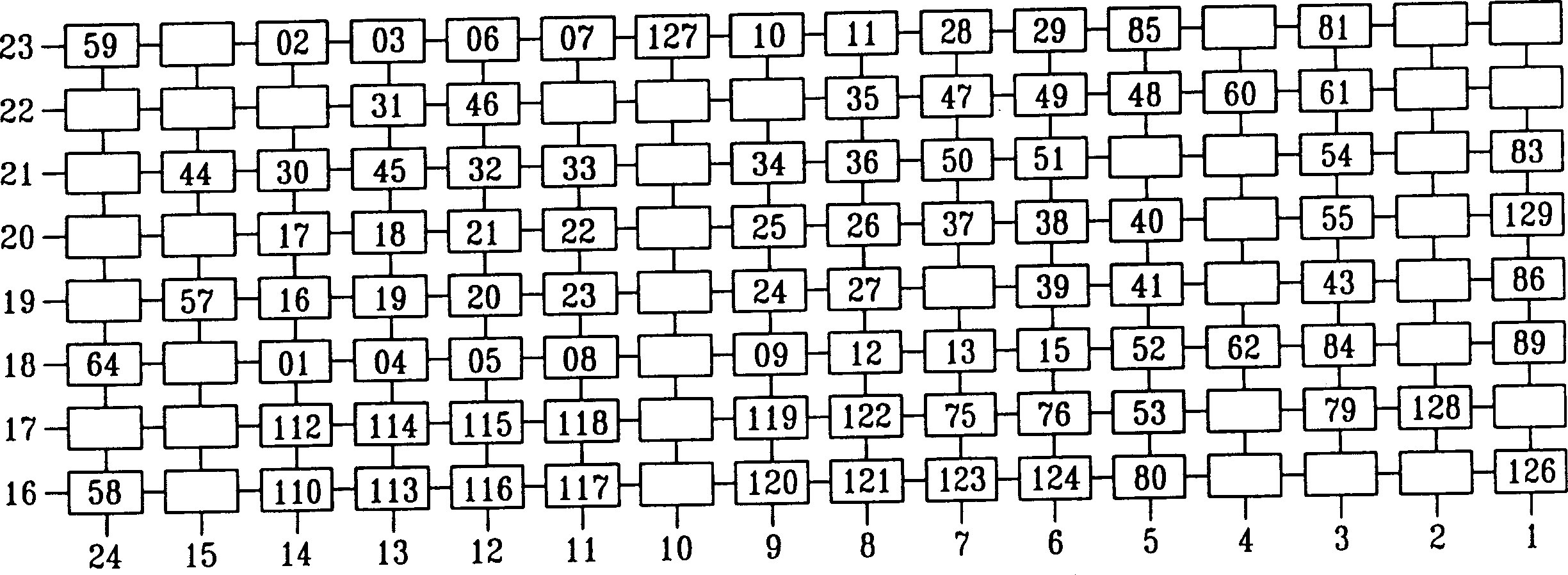
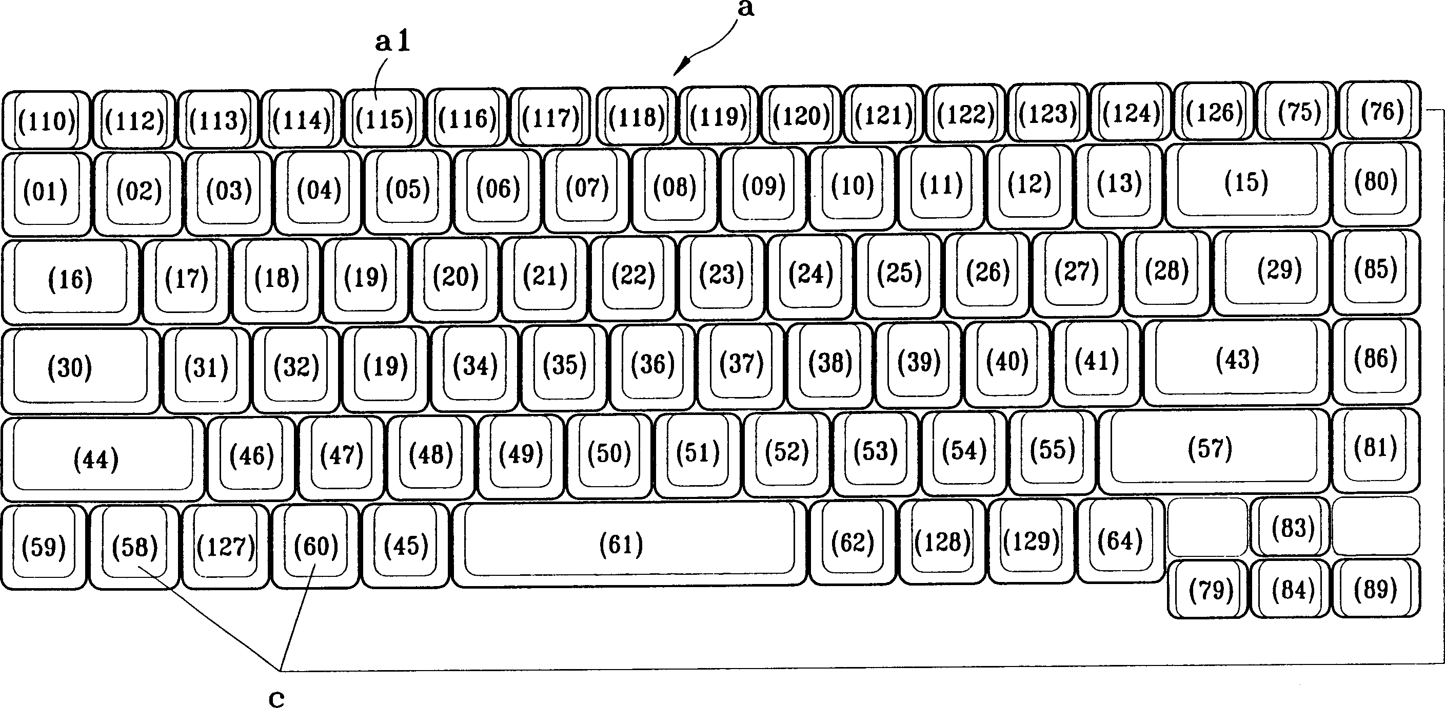
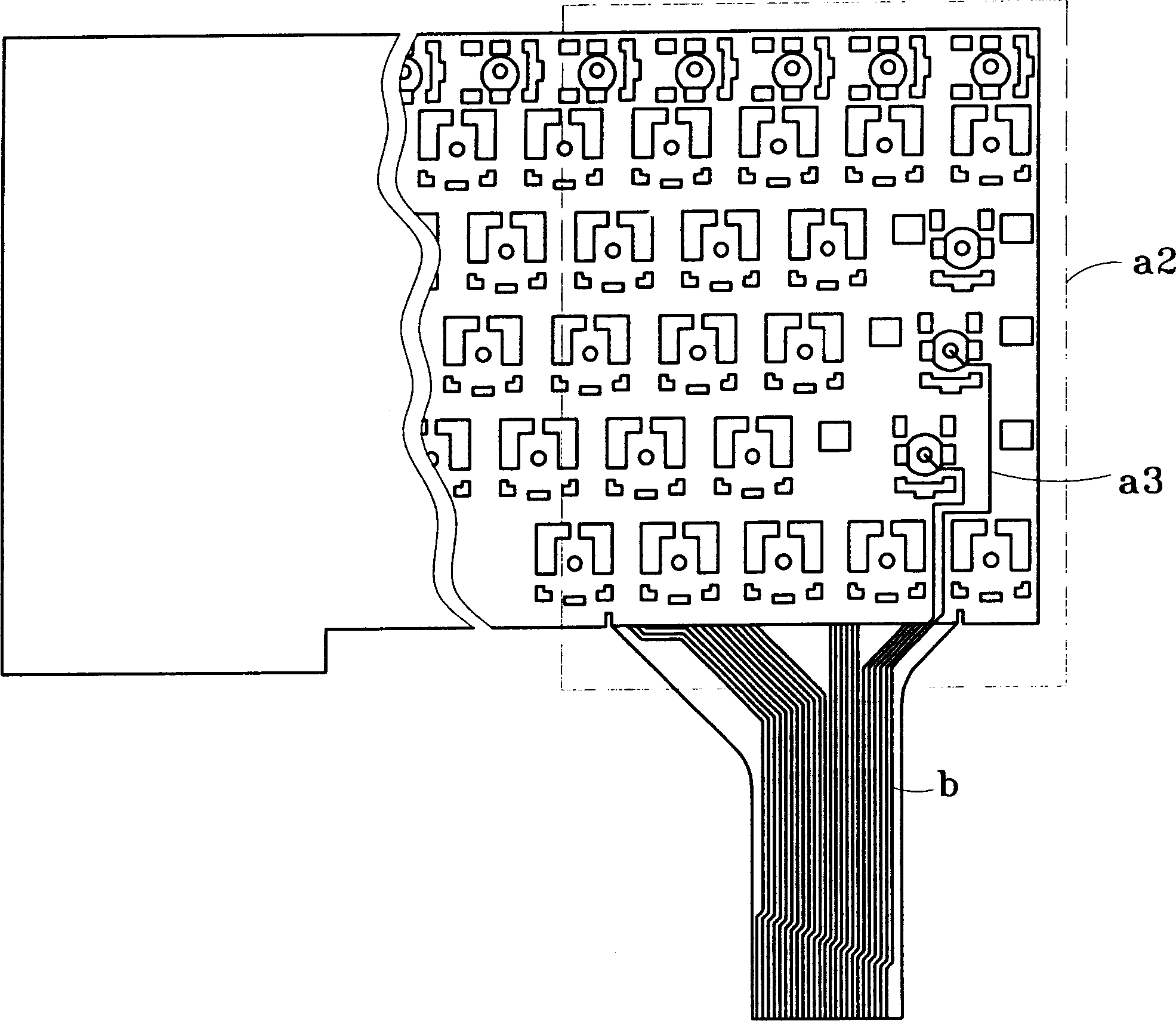
[0015] see figure 2 , 3 , is a schematic diagram of key position distribution and thin film circuit board of the present invention. As shown in the figure: the button layout method of the membrane circuit board of the present invention is mainly to consider the situation of the membrane circuit board not jumping wires and avoiding the generation of unknown key signals when the membrane circuit board is arranged or arranged (Membrane Layout). After the circuit layout (Layout), then define the matrix (Matrix) arrangement, and then provide the manufacturer to fill in the code of each key into the chip; this arrangement method can reduce the circuit board printing process, reduce production costs, and increase production. Relatively, the production steps are reduced to reduce the loss caused by the rate of defective products. At the same time, it can also avoid the micro-short circuit caused by the free circuit of the jumper part, improve the reliability of the product, and avoi...


PUM


Abstract

The key position arrangement method of the film circuit board is characterized by that under the condition of having no wire jumper and preventing production of unknown key signal the key position can be arranged, when the key positions are arranged, firstly, the adjacent keys can be centralized into a group, every group can be used for defining a key position distribution diagram, then the circuit of every key of every group can be connected on the row of wires of film circuit board, then the amount of every kind of composite keys can be defined, and in the composite keys the keys which can not be colinear or can be formed into cross-coline can be arranged on the matrix scanning line of X-axis or y-axis, and under the condition of having no wire jumper other adjacent keys can be arranged.

Description

technical field [0001] The invention relates to a method for arranging key positions of thin-film circuit boards, in particular to a kind of thin-film circuit board, which considers the situation of not jumping wires and avoiding the occurrence of unknown keys. ) arrangement, and then provide the manufacturer to fill the code of each key into the chip. Background technique [0002] It is known that the keyboards used in notebook computers currently on the market also include a thin film circuit board (Membrane) in addition to the upper keys, substrates, and bridges. When making this thin film circuit board, the manufacturer will first define and shape the button position layout, and then hand over the defined and shaped button position layout to the manufacturer for the matrix arrangement of the buttons (such as figure 1 shown), after the matrix arrangement of key positions, fill in the position code of each key in the chip. [0003] After the manufacturer arranges the mat...

Claims


Application Information

Patent Timeline
Patent Type & Authority Applications(China)
IPC IPC(8): G06F3/023
Inventor 吕添敏
Owner ZIPPY TECH
Why Eureka
Try Eureka