Optical film, diffusion chip, reflection plate, surface light source device and liquid crystal device

An optical film and light incident surface technology, which is applied in the fields of surface light source devices, liquid crystal display devices, reflectors, optical films, and diffusers, and can solve the problems of large scattering, increased cost, and limited thickness of thin surface light source devices.

Inactive Publication Date: 2004-05-19
ORMON CORP
View PDF0 Cites 13 Cited by
  • Summary
  • Abstract
  • Description
  • Claims
  • Application Information

AI Technical Summary

Problems solved by technology

[0015] However, in the above-mentioned surface light source device, the scattering of the light diffused by the diffusion sheet 3 is large, so the Figure 9 The light L diffused in the indicated direction passes through the prism sheets 4 and 5 and is emitted in an oblique direction.
Such light L constitutes a loss, so the front brightness of the surface light source device will be reduced.
[0016] Moreover, in figure 1 In the surface light source device with such a structure as shown, the diffusion sheet and the prism sheet formed separately must be stacked on the light guide plate, so there is a limit to reducing the thickness of the surface light source device.
The number of parts of the surface light source device is large, so the man-hours for assembly are increased, and the cost is increased.

Method used


Image

  • Optical film, diffusion chip, reflection plate, surface light source device and liquid crystal device
  • Optical film, diffusion chip, reflection plate, surface light source device and liquid crystal device
  • Optical film, diffusion chip, reflection plate, surface light source device and liquid crystal device

Examples


no. 1 approach

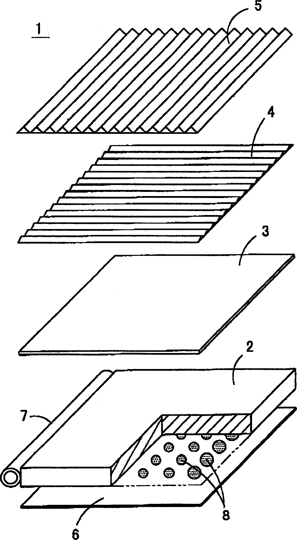
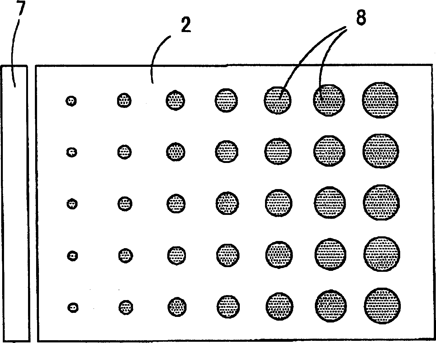
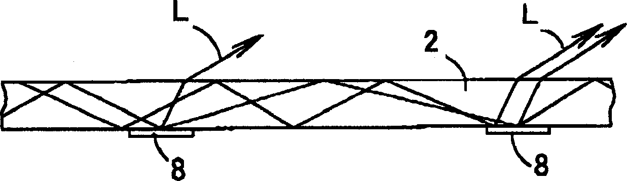
[0052] Picture 10 Is an exploded perspective view of a surface light source device 21 according to an embodiment of the present invention, Picture 11 Is its side view. The surface light source device 21 is composed of a light guide plate 22, an optical film 23 arranged on the upper surface of the light guide plate 22, a reflective plate 24 arranged under the light guide plate 22, and a light source 25 arranged on the side surface of the light guide plate 22. The light source 25 can be a light emitting diode (LED), a cold cathode ray tube, an electroluminescence (EL), etc. The light guide plate 22 is formed of a transparent resin or glass material with high refractive index such as methacrylic resin or polycarbonate resin as a flat plate. In the lower surface of the light guide plate 22, minute concave-convex patterns 26 with circular or triangular cross-sections are formed, and the distribution density of the concave-convex patterns 26 gradually increases as it moves away from ...

no. 2 approach

[0071] Figure 18 It is an exploded perspective view of a surface light source device 41 according to another embodiment of the present invention. In this surface light source device 41, an optical film 42 and a prism sheet 43 are stacked on the light guide plate 22.

[0072] The prisms 27 formed on the upper surface of the optical film 42 are in one direction, but they do not extend over the entire width of the optical film 42 but are appropriately divided and arranged on the upper surface of the optical film 42. In addition, the size of the prism 27 is not uniform, but is formed into a random size.

[0073] The diffusion patterns 28 arranged under the optical film 42 are also in the same direction. Each diffusion pattern 28 can extend over the entire width of the optical film 42, and each diffusion pattern 28 can also be appropriately divided and arranged under the optical film 42. . In addition, the diffusion patterns 28 are also formed in random sizes, but have shapes that ar...

no. 3 approach

[0077] Fig. 19(a) is a partial plan view of an optical film 45 according to still another embodiment of the present invention, Fig. 19(b) is a X1-X1 sectional view in Fig. 19(a), and Fig. 19(c) is a back view thereof , Fig. 19(d) is a cross-sectional view of X2-X2 in Fig. 19(c). The optical film 45 can be used for example Figure 18 Such a surface light source device is shown. Similarly, the prism 27 on the upper surface of the optical film 45 is appropriately divided and arranged. In addition, the size of the prism 27 is not uniform, but is formed into a random size. Furthermore, in the optical film 45, each prism 27 is divided into a tortoise shell shape, and the degree of randomness is very high.

[0078] The diffusion pattern 28 provided under the optical film 45 is also divided into tortoiseshell-shaped regions and arranged at a high degree of randomness. Furthermore, in this optical film 45, as shown in FIG. 19(b), the diffusion pattern 28 is composed of the main inclined su...


PUM

PropertyMeasurementUnit
angleaaaaaaaaaa
refractive indexaaaaaaaaaa

Abstract

Provided is an optical film having diffusion pattern capable of diffusing light while decreasing the light that is emitted in a directions other than the vertical direction to be lost, and moreover, to provide an optical film having both functions of a prism sheet and a diffusing sheet.A plurality of diffusion patterns are formed on a light incident plane of an optical film , to form a plurality of prisms on a light exit plane. At least in one section, the diffusion pattern consists of a main inclined face formed of a curved face of a relatively small inclination, and a sub-inclined face of a relatively large opposite inclination to the main inclined face .

Description

Technical field [0001] The invention relates to an optical film, a diffusion sheet, a reflecting plate, a surface light source device and a liquid crystal display device. In particular, it relates to an optical film or the like having an optical pattern formed on the surface, and also relates to a surface light source device and a liquid crystal display device using the optical film or the like. Background technique [0002] figure 1 It is a partially cut exploded perspective view of the structure of a conventional surface light source device 1 used in a liquid crystal display device and the like. In this surface light source device 1, a diffusion sheet 3 is superimposed on a light guide plate 2 made of a transparent material with a large refractive index (viewed from the observer's side), and two prism sheets 4 and 5 are superimposed on it. A reflecting plate 6 made of a white plate or the like is arranged on the underside of the light plate 2. In addition, a light source 7 co...

Claims


Application Information

Patent Timeline
Patent Type & Authority Applications(China)
IPC IPC(8): G02B6/00F21V8/00F21Y103/00G02B5/02G02B5/04G02B5/08G02F1/13357
CPCG02B5/0236G02B6/0065G02B5/0215G02B6/0053G02B6/0038G02B5/045G02B5/0257G02B5/021G02B5/0263
Inventor 松下元彦船本昭宏青山茂松井优贵川户健治
Owner ORMON CORP
Why Eureka
Try Eureka