Method for forming semiconductor component in non-implantation mode
A technology of semiconductors and components, applied in the field of forming semiconductor components by non-implantation method, which can solve the problems of difficulty in making semiconductor components, lower component qualification rate and electrical quality, and many process steps
- Summary
- Abstract
- Description
- Claims
- Application Information
AI Technical Summary
Problems solved by technology
Method used
Image

Examples
Embodiment Construction
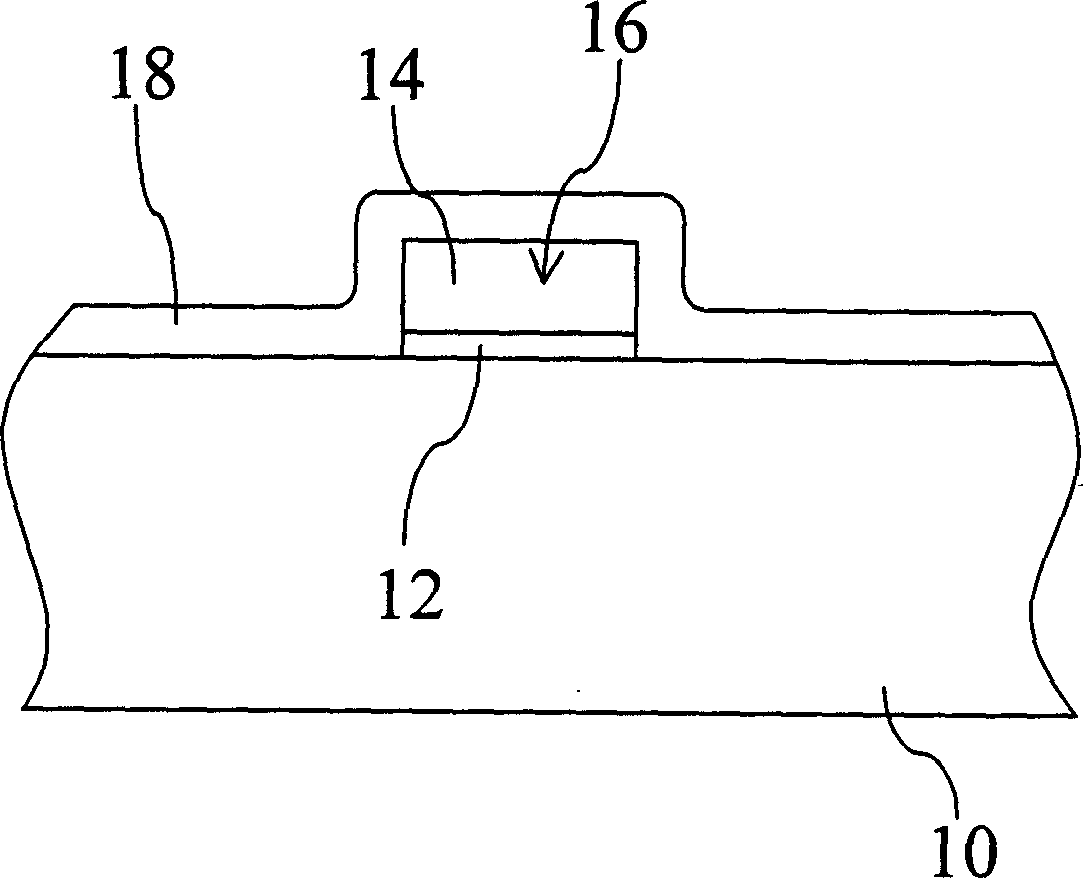
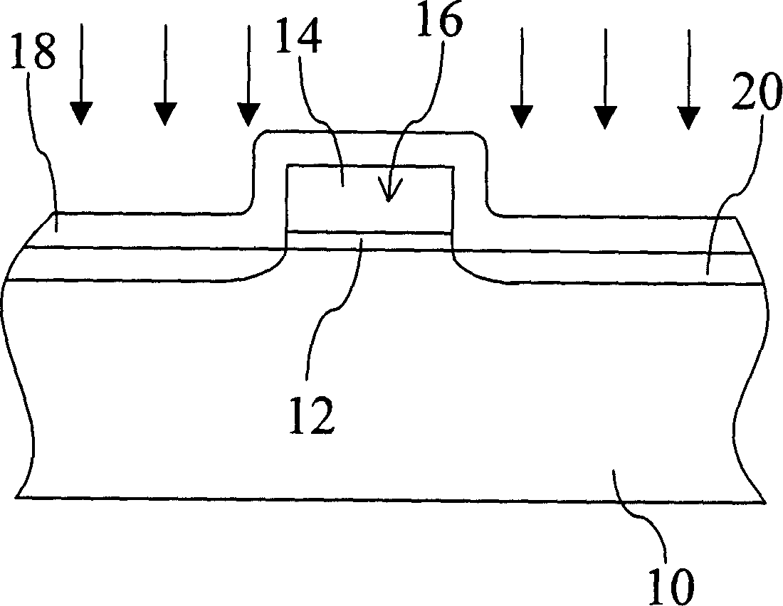
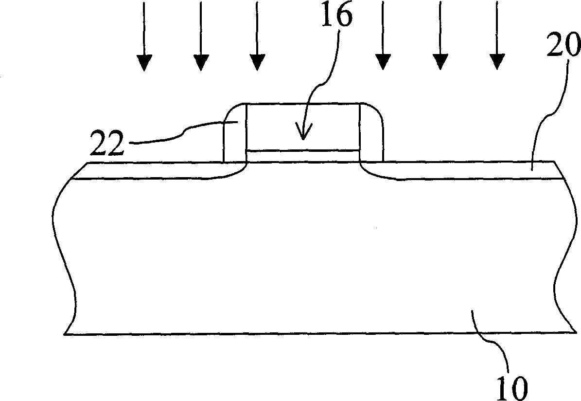
[0013] The present invention uses the non-ion implantation method of ion high-temperature drive-in (drive in) to form an ion-doped region in the semiconductor substrate to replace the known method of using secondary ion implantation and secondary thermal tempering process, so The deficiencies in the known technology can be effectively solved, and a transistor manufacturing method with few steps and simple manufacturing process is provided.
[0014] Figure 2(a) to Figure 2(e) It is a cross-sectional view of each step of making a semiconductor component in a preferred embodiment of the present invention. As shown in the figure, the manufacturing method of the present invention includes the following steps: first provide a semiconductor substrate 30, please refer to Fig. 2 (a) Form an oxide layer 32 and a polysilicon layer 34 sequentially on the surface of the semiconductor substrate 30 by chemical vapor deposition technology, and then use a lithographic etching process to etch ...
PUM
| Property | Measurement | Unit |
|---|---|---|
| Thickness | aaaaa | aaaaa |
Abstract
Description
Claims
Application Information
 - R&D
- Intellectual Property
- Life Sciences
- Materials
- Tech Scout
- Unparalleled Data Quality
- Higher Quality Content
- 60% Fewer Hallucinations
Browse by: Latest US Patents, China's latest patents, Technical Efficacy Thesaurus, Application Domain, Technology Topic, Popular Technical Reports.
© 2025 PatSnap. All rights reserved.Legal|Privacy policy|Modern Slavery Act Transparency Statement|Sitemap|About US| Contact US: help@patsnap.com