Duty ratio correction circuit

A duty cycle correction, circuit technology, applied in electrical components, generation of electrical pulses, automatic control of power, etc., can solve problems such as can not be ignored

Inactive Publication Date: 2004-06-23
PANASONIC CORP
View PDF0 Cites 27 Cited by
  • Summary
  • Abstract
  • Description
  • Claims
  • Application Information

AI Technical Summary

Problems solved by technology

The error d3 can be ignored when the frequency of clock CK0 and CK1 is relatively low, but it cannot be ignored as the frequency increases

Method used


Image

  • Duty ratio correction circuit
  • Duty ratio correction circuit
  • Duty ratio correction circuit

Examples


no. 1 example

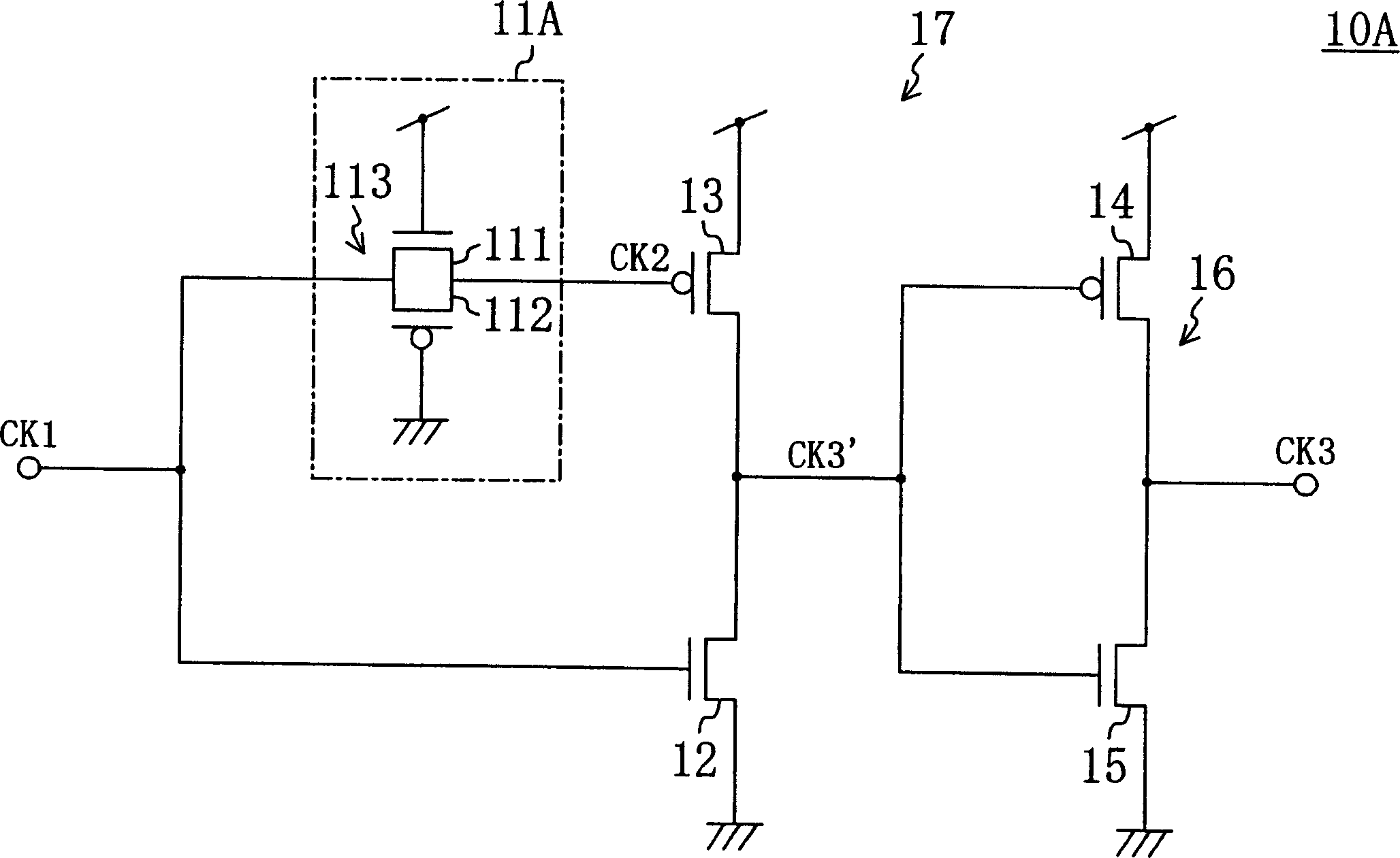
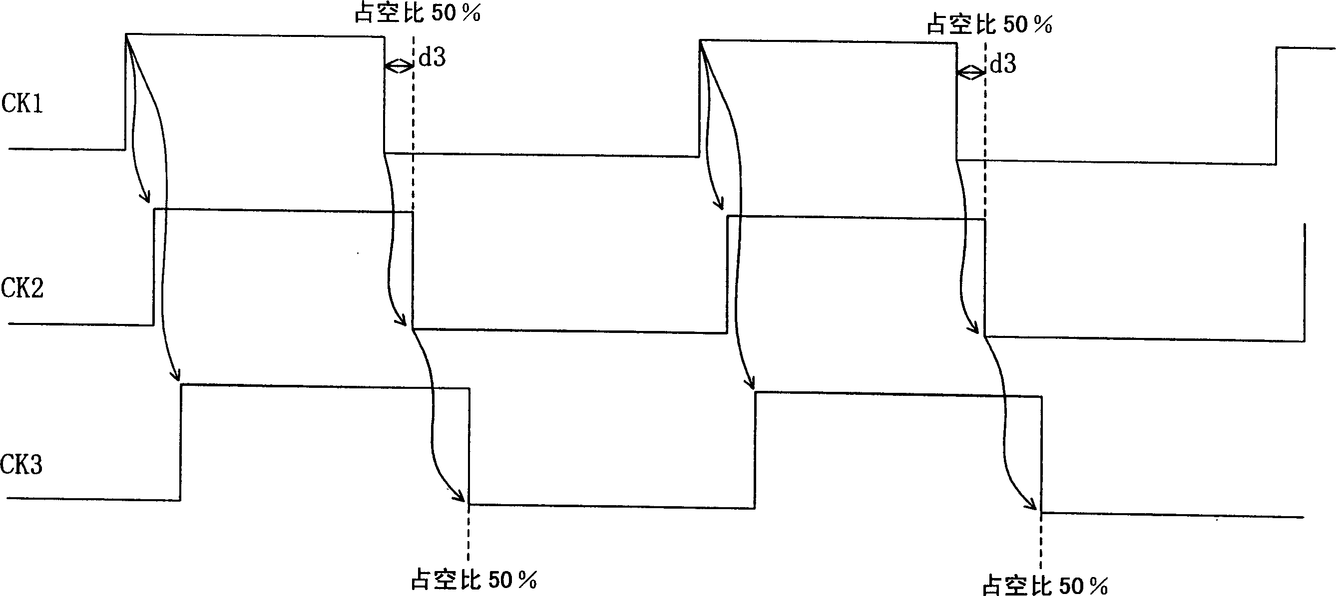
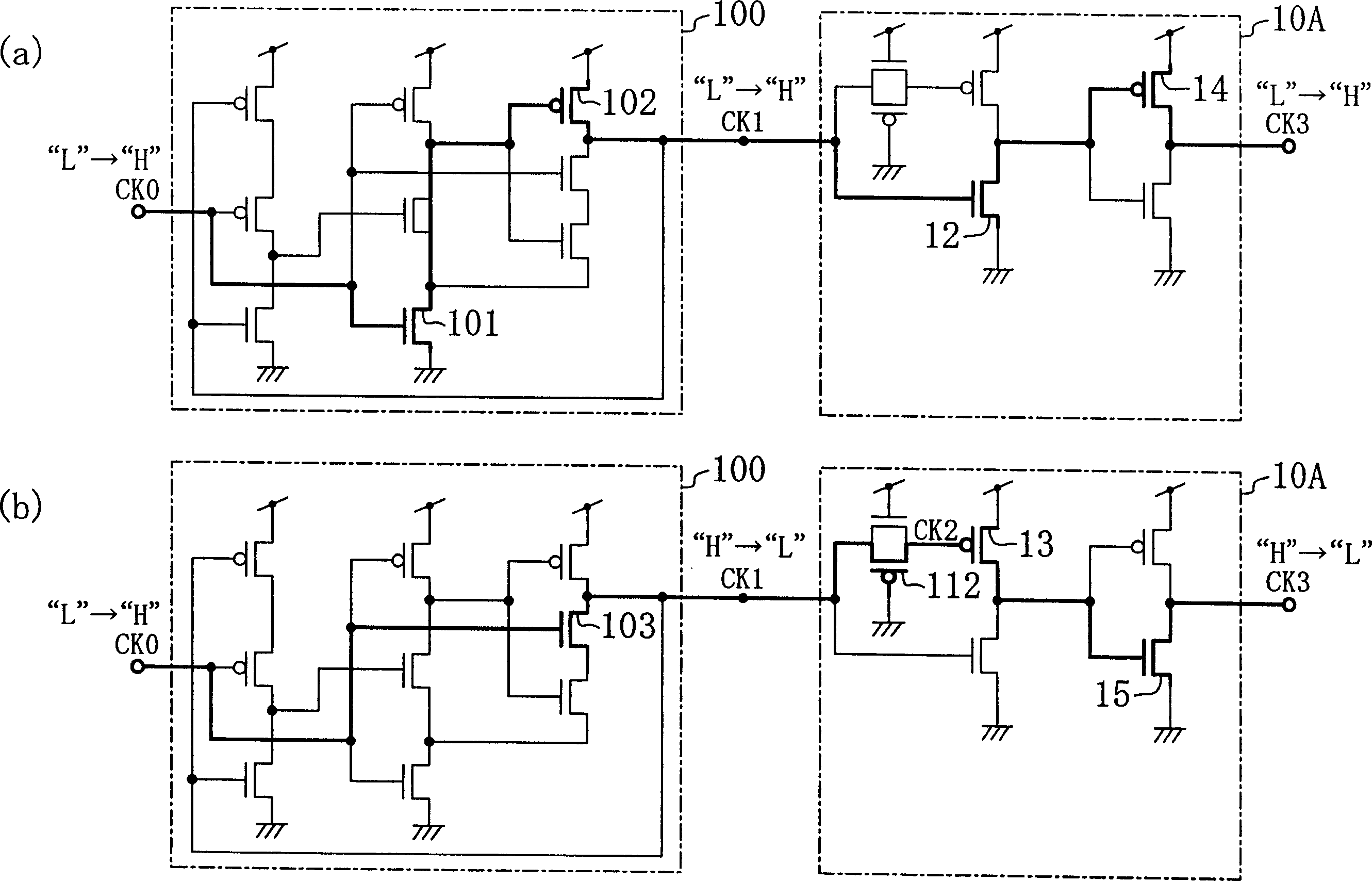
[0032] figure 1 The circuit configuration of the duty ratio correction circuit according to the first embodiment of the present invention is shown. The duty cycle correction circuit 10A of this embodiment includes: a delay unit 11A, which delays the clock CK1 (equivalent to the first clock of the present invention) input to the duty cycle correction circuit 10A and then outputs the clock CK2 (equivalent to the second clock of the present invention). ); n-channel transistor 12, whose source is supplied with ground voltage, and whose gate is supplied with clock CK1; p-channel transistor 13, whose source is supplied with supply voltage, and whose gate is supplied with clock CK2; and an inverter The circuit 16 is composed of transistors 14 and 15, and outputs the clock CK3 (equivalent to the third clock of the present invention) after the signal CK3' output from the connected drains of the transistors 12 and 13 is inverted. A clock output unit 17 is constituted by transistors 12...

no. 2 example

[0049] Figure 4 A circuit configuration of a duty ratio correction circuit according to a second embodiment of the present invention is shown. The duty ratio correction circuit 10B of the present embodiment has a circuit configuration in which the delay unit 11A in the duty ratio correction circuit 10A of the first embodiment is replaced with a delay unit 11B having a different configuration. And includes the output section 18 after omitting the inverter circuit 16 in the duty ratio correction circuit 10A, and the figure 1 The signal CK3' shown is output as a clock CK3. Moreover, in Figure 4 in, with figure 1 Components that are the same as those shown are denoted by the same symbols, and descriptions thereof are omitted. Next, the delay unit 11B will be described.

[0050] The delay unit 11B has a transmission gate 113 composed of an n-channel transistor 111 and a p-channel transistor 112 . The gate of the transistor 111 is supplied with a power supply voltage. On ...

no. 3 example

[0055] Figure 5 A circuit configuration of a duty cycle correction circuit according to a third embodiment of the present invention is shown. The duty ratio correction circuit 10C of the present embodiment is constituted by replacing the delay unit 11B in the duty ratio correction circuit 10B of the second embodiment with a delay unit 11C having a different configuration. Moreover, in Figure 5 in, with Figure 4 Components that are the same as those shown are denoted by the same symbols, and descriptions thereof are omitted. Next, the delay unit 11C will be described.

[0056] The delay unit 11C has a p-channel transistor 112 . The gate threshold voltage Vth of the transistor 112 is applied to the gate of the transistor 112 . Here, since the transistor 112 is a p-channel transistor, a voltage lower than the ground voltage is applied. Thus, by applying the gate threshold voltage Vth to the gate of the transistor 112, the transistor 112 can be turned into a switching ope...


PUM


Abstract

Provided is a duty cycle correction circuit for correcting a duty cycle of an imparted clock to obtain a clock whose duty cycle is 50%. A duty cycle correction circuit is provided with: a delay part 11A for delaying a clock CK1 to output a clock CK2; and a clock output part 17 composed of transistors 12, 13 with the clocks CK1, CK2 as respective gate inputs, and an inverter circuit 16 for inverting a signal CK3' which is a common drain output of the transistors to output a clock CK3. The delay part 11A delays the clock CK1 so that the falling change of the clock CK1 may appear at a timing of duty cycle 50%. The transistors 12, 13 output a ground voltage and a power supply voltage from their common drain in accordance with the rising change of the clock CK1 and the falling change of the clock CK2 (signal CK3'). The clock CK3 whose duty cycle is finally corrected to about 50% is then obtained.

Description

technical field [0001] The present invention relates to a clock processing circuit in a digital circuit, and particularly relates to a circuit technology very suitable for correcting the duty cycle of a clock generated by a frequency division circuit or the like. Background technique [0002] In a digital circuit, it is very important to keep the duty cycle of the clock used at 50% in order to make the work of each department consistent. Typically, a clock with a 50% duty cycle is generated by a divider circuit. [0003] Figure 7 Shows the circuit configuration of a general frequency division circuit (2 frequency division circuit). The frequency division circuit 100 shown in the figure receives the input clock CK0, divides it by 2, and outputs the clock CK1. By dividing the frequency of the clock CK0 by 2, the period in which the logic value of the clock CK1 is "H" and the period in which the logic value is "L" are both one cycle time of the clock CK0. Thus, a clock CK1 ...

Claims


Application Information

Patent Timeline
Patent Type & Authority Applications(China)
IPC IPC(8): G06F1/10H03K3/017H03K5/04H03K5/13H03K5/156H03L7/093
CPCH03K5/133H03K5/1565
Inventor 道正志郎柳沢直志外山正臣梅原启二朗
Owner PANASONIC CORP
Why Eureka
Try Eureka