Testing method for substandard products of integrated circuits

A technology of integrated circuit and detection method, which is applied in the direction of electronic circuit testing, semiconductor/solid-state device testing/measurement, etc., which can solve the problems of slow inspection speed, reduced reliability, unsuitable for large-scale device detection, etc., and achieve fast detection speed and automation The effect of detection accuracy

Inactive Publication Date: 2004-07-07
DELTA ELECTRONICS INC
View PDF0 Cites 1 Cited by
  • Summary
  • Abstract
  • Description
  • Claims
  • Application Information

AI Technical Summary

Problems solved by technology

However, these two methods have the following disadvantages in actual use: In terms of online inspection, only structural defects can be inspected and the inspection speed is slow, so they are not suitable for large-scale devices on the entire wafer (large size device) detection; as far as the DC electronic probe test is concerned, when the detected integrated circuit is composed of many electronic components (such as transistors) connected in parallel, such as the above-mentioned RF power amplifier, because the probe cannot Distinguishing the drift of DC amplification from the failure or open circuit of electronic components (such as transistors), it is often misjudged as normal. Although the result of this misjudgment will not completely damage the integrated circuit in a short period of time, however, for a long time down will shorten the life cycle of the device and reduce its reliability
Therefore, it is impossible to effectively and thoroughly detect defective products only by using the above online inspection and DC electronic probe testing methods

Method used


Image

  • Testing method for substandard products of integrated circuits
  • Testing method for substandard products of integrated circuits
  • Testing method for substandard products of integrated circuits

Examples


Embodiment Construction

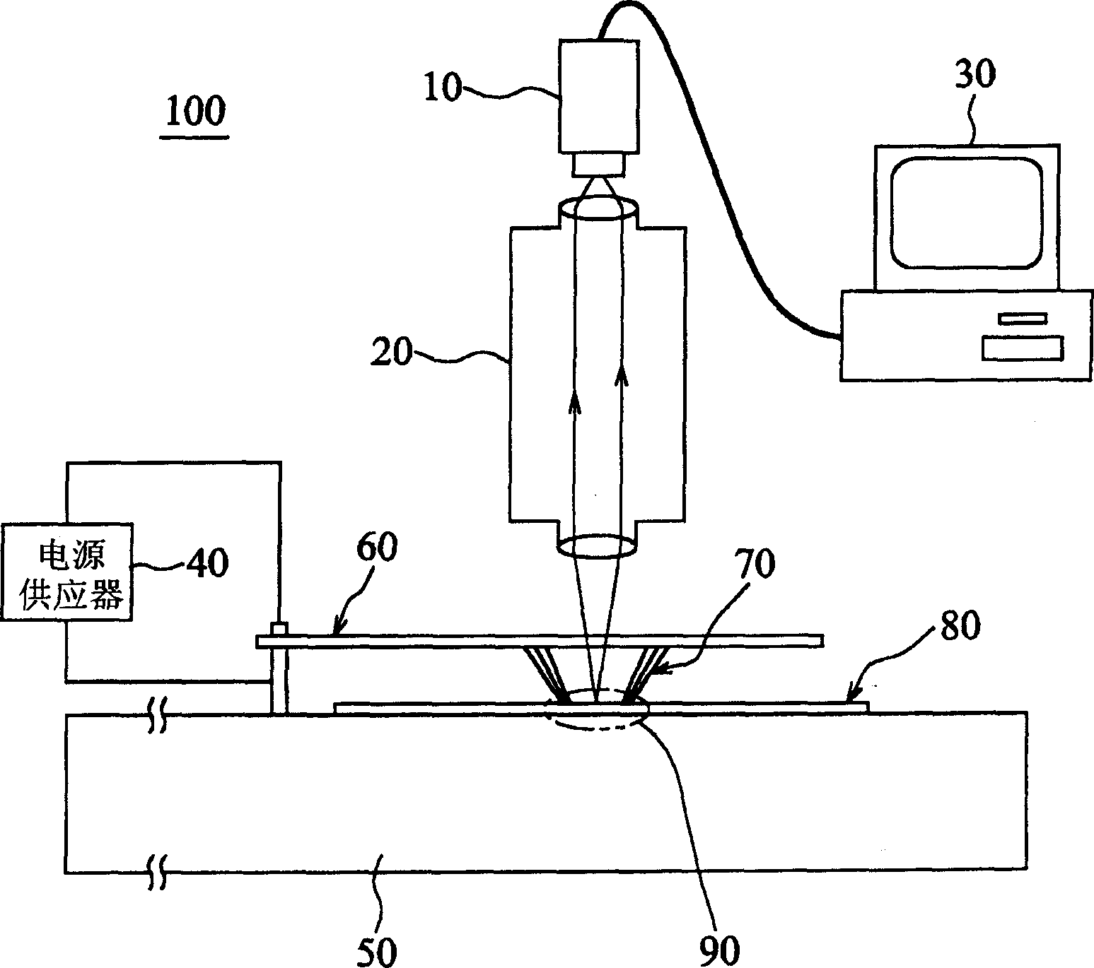
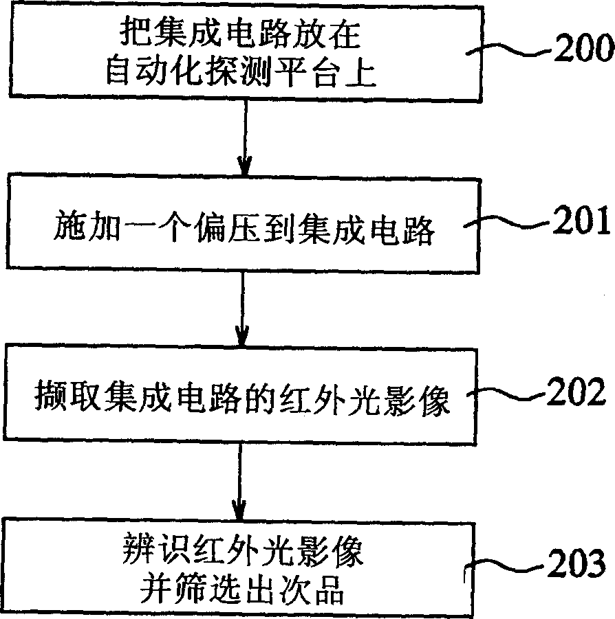
[0028] The structure, features, and functions of the detection method for defective integrated circuits of the present invention will be described in detail below with the accompanying drawings and embodiments.

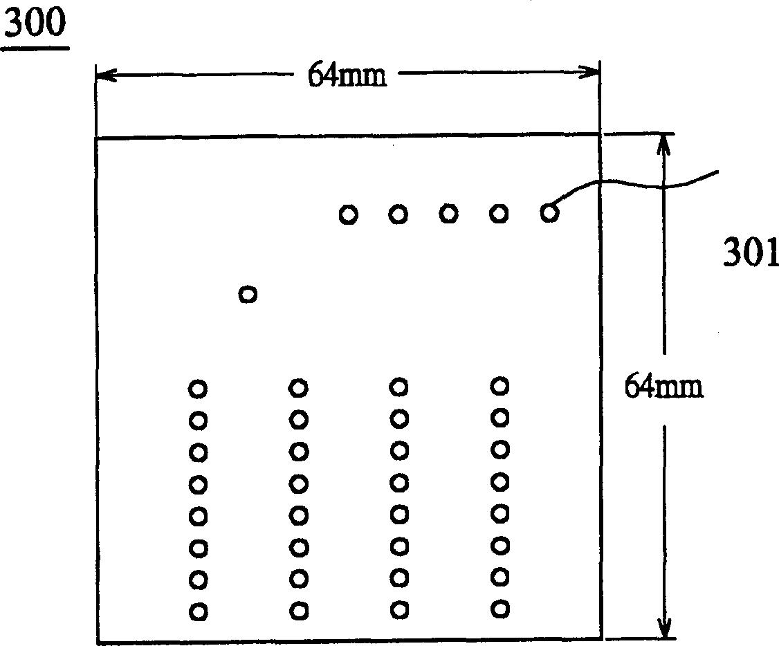
[0029] As mentioned earlier, the radio frequency power amplifier in the handheld phone is a large array of transistor cells configured by dozens of transistors in parallel. These transistors are mainly silicon bipolar transistors and gallium arsenic metal-semiconductor fields. MESFET (galliumarsenide metal-effect-semiconductor field effect transistor; MESFET) and gallium arsenide heterojunction bipolar transistor (HBT). When the gallium arsenide heterojunction bipolar transistor is energized, its The base region will have the phenomenon of radiative recombination, that is, it will emit infrared-red light. Therefore, the present invention uses the infrared light image display device to detect the integrated circuit to search for defective products in the integrated circuit...


PUM


Abstract

The present invention is a method for detecting defectives of integrated circuit ( IC ) consisting of a plurality of parallel transistors on a wafer. The method comprises the following steps: applying a bias to the transistors; and extracting the infrared imagery of the transistors. 200 placing IC on automatic detecting table 201 applying a bias to IC 202 extracting infrared imagery of IC 203 discriminating infrared imagery and rejecting defectives.

Description

Technical field [0001] The present invention relates to a method for detecting defective integrated circuits; in particular, it relates to a method for removing defective integrated circuits composed of transistors from the wafer level and packaging stage in the semiconductor process by using the principle of infrared photothermal induction. level). Background technique [0002] One of the key electronic components of the handset is the radio frequency power amplifier (RFPA). The radio frequency power amplifier is usually composed of dozens of transistors arranged in parallel to form a large transistor cell array (large transi stor cell array) to increase its output power. At present, the integrated circuits of such large transistor cell arrays are usually performed by the methods of visual in-line inspection and DC electrical probing test in the wafer stage and packaging stage of the semiconductor manufacturing process. Test to find defective products (defective). However, these...

Claims


Application Information

Patent Timeline
Patent Type & Authority Applications(China)
IPC IPC(8): G01R31/28H01L21/66
Inventor 吴建华胡政吉施盈舟黄忠谔
Owner DELTA ELECTRONICS INC
Why Eureka
Try Eureka