Physic design method for analog and radio frequency integrated circuit

A radio frequency integrated circuit and physical design technology, applied in circuits, electrical digital data processing, computing, etc., can solve the problems that engineers are difficult to correctly give layout constraints, consume a lot of time, and slow automatic design, and achieve the most The effect of optimal wiring, small parasitic effect, and area optimization

Inactive Publication Date: 2004-07-07
AIKESAILI MICROELECTRONICS TECH BEIJING
View PDF0 Cites 22 Cited by
  • Summary
  • Abstract
  • Description
  • Claims
  • Application Information

AI Technical Summary

Problems solved by technology

Therefore, in order to reduce the design cost and market risk of integrated circuits, the automation of physical layout design of integrated circuits has always been the goal pursued by the industry, because the basic gate circuit structure of digital integrated circuits is relatively simple and relatively regular, and layout parasitics should affect circuit performance. It is relatively small, and its physical layout design is relatively simple and regular, so it is easy to realize its physical layout design automation. At present, the physical layout design automation technology of digital integrated circuit circuits is relatively mature, and has been applied to actual design on a large scale In the process, this significantly improves the efficiency of the physical layout design of digital integrated circuits; compared with digital integrated circuits, the structure of analog and radio frequency integrated circuits is ever-changing, and the physical layout parasitic effects have a great impact on the performance of the circuit. The physical layout design needs Considering many requirements such as device matching, functional block matching, device symmetry, functional block symmetry, connection matching, and connection symmetry can ensure that the performance of the circuit meets the design requirements. Therefore, it is very difficult to automate the physical layout design of analog and radio frequency integrated circuits. So far, analog and The physical layout design automation technology of radio frequency integrated circuits is still in the exploratory stage, and mature automatic design methods have not yet appeared
Integrated circuit design is developing in the direction of chip circuit systems, and there are fewer and fewer

Method used


Image

  • Physic design method for analog and radio frequency integrated circuit
  • Physic design method for analog and radio frequency integrated circuit
  • Physic design method for analog and radio frequency integrated circuit

Examples


Embodiment Construction

[0040] The present invention will be further described below in conjunction with the following non-limiting examples and accompanying drawings.

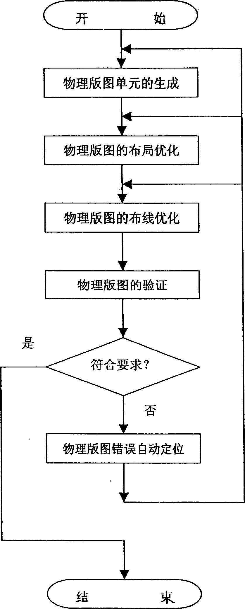
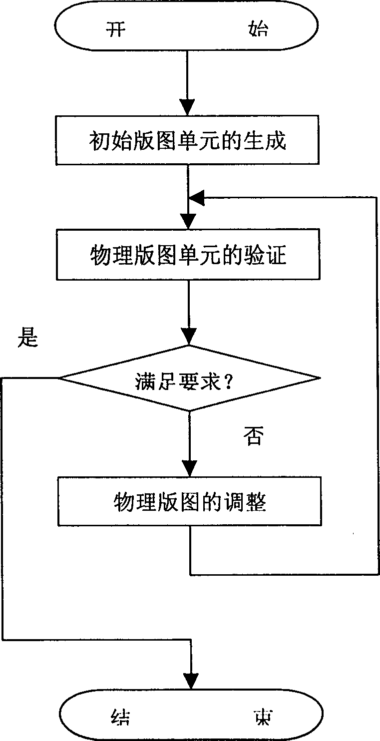
[0041] From figure 1 It can be seen that the steps of the physical design method of analog and radio frequency integrated circuits include: ① generation of physical layout cells, ② layout of physical layout, ③ routing of physical layout, ④ verification of physical layout, ⑤ automatic positioning of physical layout errors.

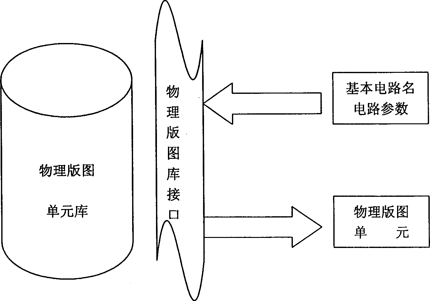
[0042] Among them, the step of step ① physical layout unit generation provides the necessary physical layout units for each unit circuit necessary for subsequent layout; the layout of step ② physical layout is mainly based on the layout requirements obtained by circuit analysis for the physical layout units provided earlier. Carry out accurate position placement; step ③ physical layout layout is mainly to connect the layout units with metal wires in the physical layout results provided above according to the layou...


PUM


Abstract

The present invention is a method for generating automatically the physical patterns of the analog and RF integrated circuits, extracting the pattern circuits, verifying the pattern circuits and positioning the pattern errors of the same. The object of the invention is to design the physical patterns of the analog and RF integrated circuits as automatically as possible, avoid the constraint condition by manual analysis and avoid the circulation of distributing-extracting-verifying. The invention comprises the following steps: generating the physical pattern unit, distributing the physical pattern, wiring the physical pattern, verifying the physical pattern and positioning automatically the physical pattern error. The invention uses the integrated physical pattern unit generator and physical pattern database interface to provide the physical pattern unit; uses the distributing technology based on signal flow to optimize the area and the property of pattern; adjusts automatically the extracting accuracy of pattern parasitic parameters to increase the extracting speed; uses the macro-model to increase the emulating speed and the capacity of circuit and uses the emulation comparing technology to position the pattern error.

Description

technical field [0001] The present invention relates to a kind of physical design method of analog and radio frequency integrated circuit, more specifically, the present invention relates to the automatic generation of circuit unit physical layout of analog and radio frequency integrated circuit, automatic generation of circuit physical layout, rapid extraction of layout circuit, layout circuit Fast verification and location of layout errors. technical background [0002] The physical layout design of integrated circuits is an important part of the entire integrated circuit design process. It affects the design cost of the entire integrated circuit product. The improvement of the efficiency of physical layout design can shorten the time to market of integrated circuit products, reduce design costs and market risks. An important means to improve the efficiency of physical layout design is the automation of physical layout design. Therefore, in order to reduce the design cost...

Claims


Application Information

Patent Timeline
IPC IPC(8): G06F17/50H01L21/82H01L27/00
Inventor 张鹏飞张锡盛吴玉平
Owner AIKESAILI MICROELECTRONICS TECH BEIJING
Why Eureka
Try Eureka