Method for maknkig shallow trench isolation zone
A manufacturing method and technology of shallow ditches, applied in semiconductor/solid-state device manufacturing, electrical components, circuits, etc., can solve problems such as inability to master the manufacturing process and inability to achieve machine self-testing, so as to achieve improved detection capabilities and low cost , the effect of simple method
- Summary
- Abstract
- Description
- Claims
- Application Information
AI Technical Summary
Problems solved by technology
Method used
Image

Examples
Embodiment Construction
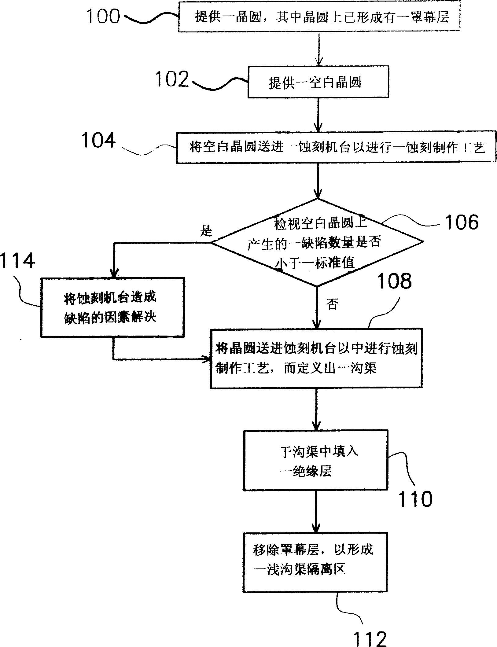
[0017] figure 1 As shown, it is a flow chart of forming a shallow trench isolation region according to a preferred embodiment of the present invention.
[0018] Please refer to figure 1 , first provide a wafer (step 100), this wafer can also be referred to as a product wafer, wherein a mask layer has been formed on this wafer, and it is subsequently used as an etching mask when patterning the wafer screen. In this embodiment, a pad oxide layer is further formed between the mask layer and the wafer to protect the surface of the wafer, and the material of the mask layer is, for example, silicon nitride.
[0019] At the same time, a blank wafer is provided (step 102 ), wherein no photoresist layer, mask layer and other film layers are formed on the blank wafer.
[0020] Then, before performing an etching process on the wafer to define the trenches, the blank wafer is sent into an etching tool to perform an etching process (step 104 ). The etching process includes an etching r...
PUM
 Abstract
Description
Claims
Application Information
 - Generate Ideas
- Intellectual Property
- Life Sciences
- Materials
- Tech Scout
- Unparalleled Data Quality
- Higher Quality Content
- 60% Fewer Hallucinations
Browse by: Latest US Patents, China's latest patents, Technical Efficacy Thesaurus, Application Domain, Technology Topic, Popular Technical Reports.
© 2025 PatSnap. All rights reserved.Legal|Privacy policy|Modern Slavery Act Transparency Statement|Sitemap|About US| Contact US: help@patsnap.com