Method of mfg. semiconductor device for improving adhesion property of copper metalic butt barrier layer

A semiconductor and copper metal technology, applied in the field of manufacturing semiconductor devices with copper metal layers, can solve problems such as fracture, peeling, defective lines, etc., to prevent adhesion decline, prevent stress-induced voids, and prevent stress migration and electron migration decrease the effect of

Inactive Publication Date: 2004-08-11
RENESAS ELECTRONICS CORP
View PDF1 Cites 9 Cited by
  • Summary
  • Abstract
  • Description
  • Claims
  • Application Information

AI Technical Summary

Problems solved by technology

[0009] Furthermore, the extreme decrease in the adhesion of the copper metal layer 116 to the barrier metal can cause the copper metal layer 116 to peel off, resulting in defective lines, and thus broken lines.

Method used


Image

  • Method of mfg. semiconductor device for improving adhesion property of copper metalic butt barrier layer
  • Method of mfg. semiconductor device for improving adhesion property of copper metalic butt barrier layer
  • Method of mfg. semiconductor device for improving adhesion property of copper metalic butt barrier layer

Examples


Embodiment Construction

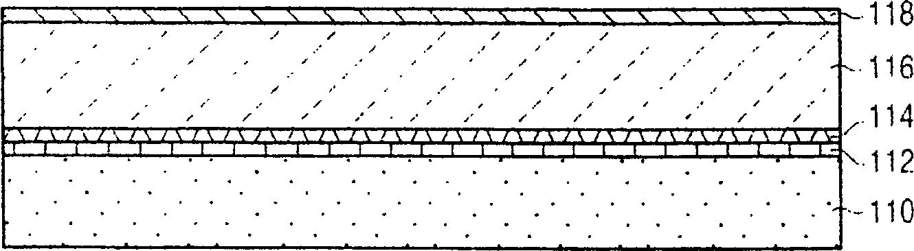
[0016] in such as Figure 2A After forming an unillustrated semiconductor element on the shown semiconductor substrate 10, a 100-300 nm thick oxide film (SiO 2 film), as an interlayer insulating film. In SiO 2 A SiCN film 14 with a thickness of 10-150 nm is formed on the film 12 as an etching limiting film to improve the processability of the circuit. Further, on the SiCN film 14, SiO with a thickness of 100-1800 nm is formed. 2 The film 16, as an insulating film, is used to form wiring. Hereinafter, the SiCN film serving as an etching limiting film is referred to as a "limiting SiCN film". Also, in the process of forming semiconductor elements such as transistors, resistors, capacitors, etc., and wiring for connecting the semiconductor elements later on the semiconductor substrate, the semiconductor substrate including these semiconductor elements formed thereon is collectively referred to as " chip".

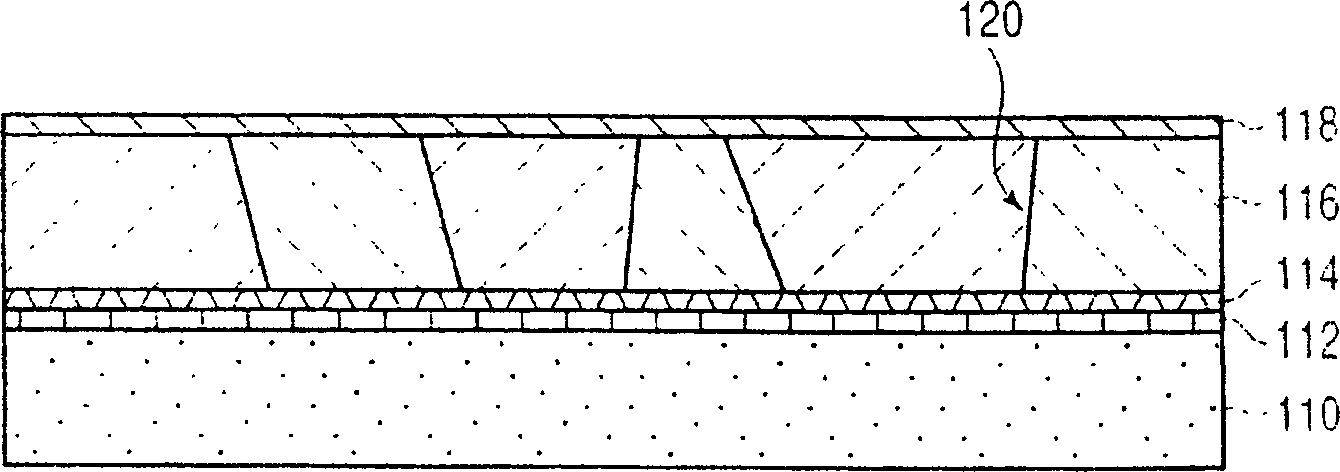
[0017] Subsequently, in the photolithography process on the SiO 2 ...


PUM


Abstract

A method of manufacturing a semiconductor device according to the present invention forms a laminate metal film having a copper metal layer and a barrier metal, and once immerses the laminate metal film in a solution including an organic acid having at least one carboxyl group before a heat treatment, thereby removing from the laminate metal film an oxide which is the source of oxygen that diffuses during the heat treatment.

Description

technical field [0001] The present invention relates to a method of manufacturing a semiconductor device with a copper metal layer, wherein the copper metal layer is a metal layer mainly containing copper. Background technique [0002] In general, it is difficult to etch copper metal. This necessitates the use of damascene-based line formation techniques to form copper metal layers, as opposed to forming lines by etching aluminum. The Damascene method is disclosed, for example, in JP-2001-156168-A as follows. After forming a groove for wiring in the insulating film, a barrier metal, a seed layer, and a copper metal layer that later serve as a barrier layer for preventing copper diffusion are sequentially formed. Subsequently, copper grain growth annealing for growing copper grains is performed, followed by a CMP (Chemical and Mechanical Polishing) process to polish the copper metal layer until the insulating film is exposed and copper lines are formed in the grooves. [0...

Claims


Application Information

Patent Timeline
Patent Type & Authority Applications(China)
IPC IPC(8): H01L21/3205H01L21/02H01L21/306H01L21/321H01L21/3213H01L21/44H01L21/4763H01L21/768H01L23/52
CPCH01L21/76877H01L21/02074
Inventor 冈田纪雄
Owner RENESAS ELECTRONICS CORP
Why Eureka
Try Eureka